
Page 198 - Sami Franssila Introduction to Microfabrication
P. 198
Bonding and Layer Transfer 177
+
+
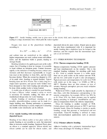
Glass Na Na Na +
O 2− O 2− O 2−
<Si> anode
−300 ... −1000 V
Heater block, 300−500°C
Figure 17.7 Anodic bonding: mobile ions in glass move in the electric field, and a depletion region is established,
leading to a large electrostatic force which pulls the wafers together
Oxygen ions react at the glass/silicon interface deposited silicon for glass wafers. Doped spin-on glass
according to has also been experimented with. It is important for
anodic bonding that a depletion layer be formed at the
Si + 2O 2− −→ SiO 2 + 4e − (17.4) interface, and this requires that the intermediate layer
acts as an ion barrier.
and sodium ions are neutralized at the cathode. If
higher temperatures are used, sodium atoms will diffuse
faster, and the depletion width is greater, leading to 17.3 OTHER BONDING TECHNIQUES
stronger bonds.
17.3.1 Thermo-compression bonding (TCB)
Bonding initiation is by applying pressure at the wafer
centre, but, if bonding is done in vacuum, it is possible Thermo-compression bonding (TCB) applies pressure
to bond without an initiation point. Current increases and heat simultaneously on the samples. This is the
rapidly at the initiation of bonding because contact area standard bonding technique for attaching gold leads
increases and then decreases exponentially as oxygen to ICs. Gold is suitable because it is noble metal:
ions react at the interface to form SiO 2 , and the oxide there are no gold oxides on the surface prevent TCB,
becomes thicker. When the current has dropped to 10% and the low yield point of gold is also advantageous.
of its peak value, bonding is termed finished. Typical Typical pressures and temperatures for wafer level TCB
bonding times are 10 to 30 min. This is fairly long for a with metals are in the range 1 to 10 MPa at 300 to
single-wafer operation, and special wafer holders have 400 C. Bonding times are then minutes or tens of
◦
been designed so that wafer loading and unloading can minutes. Nitrogen atmosphere prevents metal oxidation
be done while another wafer is being bonded. during bonding.
A sizable area of silicon is needed for good bonding. Wafer-level TCB is made possible by deposition of
At least a 200 µm ‘collar’ around a cavity or recess thin films, with film thicknesses corresponding to the
is necessary for hermetic sealing, but there are no eutectic composition, for example, 80%wt Au, 20% Sn
standardized design rules for wafer bonding. or Si 3%wt, 97% Au. Static pressure may be applied
Anodic bonding of multilayer structures is also during annealing in hydrogen. Interdiffusion can take
possible: glass/silicon/glass systems can be made in a place at temperatures below the eutectic temperature.
single bonding step. Heating uniformity is important, Glass–frit bonding is another example of TCB.
and double side heating is usually employed. Contacting Certain glasses melt under pressure at 500 C and form
◦
the middle wafer electrically can be difficult. hermetic bonds. Glass-frit bonding is similar to anodic
bonding, except that pressure is mechanical and not
electrostatic. Glass-frit bonding is utilized in many
17.2.1 Anodic bonding with intermediate
bulk micromechanical applications such as pressure
deposited layers
sensors.
Bonding of two silicon wafers or two glass wafers by
anodic bonding is not possible as such, but deposited
17.3.2 Polymer adhesive bonding
films in between enable bonding. Sputtered Pyrex glass
on silicon is a standard approach. Silicon nitride and Adhesive bonding with a polymeric intermediate layer
silicon carbide can be used for silicon wafers, and offers many advantages for bonding as follows: