
Page 195 - Sami Franssila Introduction to Microfabrication
P. 195
174 Introduction to Microfabrication
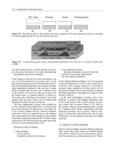
RCA-1 clean RT joining Anneal Thinning (optional)
(a) (b) (c) (d)
Figure 17.1 Prototypical steps in wafer bonding (a) surface preparation; (b) room temperature joining; (c) annealing
for bond strengthening and (d) top wafer thinning (optional)
0.8-µm CMOS integrated circuit Pads
Cap glass
Frame Seismic mass Frame
Folded thin beam structure Bottom glass
Figure 17.2 Accelerometer by glass–silicon–glass bonding. Reproduced from Takao, H. et al. (2001), by permission
of IEEE
• in device processing as a process step like any other; – room temperature joining
• at the end of the process for cavity formation and initiation of bonding at centre or wafer flat
encapsulation (zero-level packaging). – anneal for bond energy improvement
– top wafer thinning (optional).
If the bonding is done by the wafer manufacturer, the
user sees the bonded wafer as any other wafer, except In microturbine fabrication (Figure 1.10), five structured
that its special properties will be utilized in the process. wafers are bonded one at a time to form a final device.
Silicon-on-insulator technology is an example of bonded In blanket wafer bonding, alignment is trivial but in
wafer application (bonding is only one way to make structured wafer bonding it is critical, and it will be
SOI). In bonded SOI, the top wafer is thinned down discussed in Chapter 28. No wafer thinning is required
to 10 to 50 µm. It is known as the device wafer, and for turbine application: blade thickness is equal to wafer
the bottom wafer, of standard thickness, is known as thickness, 380 µm.
the handle wafer. Bonding is not limited to two-wafer In the final encapsulation, bonding serves many
joining. More and more wafers can be bonded, yield functions: it protects free-standing mechanical parts
allowing. Of course, the price will go up. in the dicing process and it forms cavities for pres-
The basic requirements for good wafer bonding are sure sensors and resonators (Figure 17.2). With all
(1) the materials being bonded form a chemical bond the sensitive, delicate micromechanical parts covered
across their interface, (2) high stresses are avoided and by a capping wafer, dicing, encapsulation and other
(3) no interface bubbles develop. Thermal expansion packaging operations can be generic, whereas pack-
coefficients of the two materials have to be matched aging of unprotected chips with beams and air gaps
and various glasses have been tailored to match silicon would have to be developed for each and every design
coefficients of thermal expansion CTE. To achieve these separately.
requirements, the following processing steps are usually
involved in wafer bonding (Figure 17.1).
17.1 SILICON FUSION BONDING
Prototypical steps in bonding:
Silicon-to-silicon bonding can yield abrupt pn-junctions
– surface cleaning when p-type and n-type wafers are bonded without
particle removal oxide. This is utilized in power semiconductor fabrica-
hydrophilic surface finish treatment tion. The alternatives are epitaxial deposition of 100 µm