
Page 191 - Sami Franssila Introduction to Microfabrication
P. 191
170 Introduction to Microfabrication
4
2
4
2
4
2
3 3 3 c
<001> 2
1 1 1 1
<110>
W d
<110> Si substrate
(a) (b)
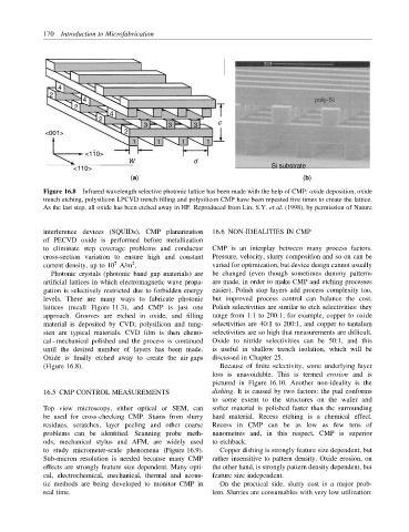
Figure 16.8 Infrared wavelength selective photonic lattice has been made with the help of CMP: oxide deposition, oxide
trench etching, polysilicon LPCVD trench filling and polysilicon CMP have been repeated five times to create the lattice.
As the last step, all oxide has been etched away in HF. Reproduced from Lin, S.Y. et al. (1998), by permission of Nature
interference devices (SQUIDs), CMP planarization 16.6 NON-IDEALITIES IN CMP
of PECVD oxide is performed before metallization
to eliminate step coverage problems and conductor CMP is an interplay between many process factors.
cross-section variation to ensure high and constant Pressure, velocity, slurry composition and so on can be
2
7
current density, up to 10 A/m . varied for optimization, but device design cannot usually
Photonic crystals (photonic band gap materials) are be changed (even though sometimes dummy patterns
artificial lattices in which electromagnetic wave propa- are made, in order to make CMP and etching processes
gation is selectively restricted due to forbidden energy easier). Polish stop layers add process complexity too,
levels. There are many ways to fabricate photonic but improved process control can balance the cost.
lattices (recall Figure 11.3), and CMP is just one Polish selectivities are similar to etch selectivities: they
approach. Grooves are etched in oxide, and filling range from 1:1 to 200:1; for example, copper to oxide
material is deposited by CVD; polysilicon and tung- selectivities are 40:1 to 200:1, and copper to tantalum
sten are typical materials. CVD film is then chemi- selectivities are so high that measurements are difficult.
cal–mechanical polished and the process is continued Oxide to nitride selectivities can be 50:1, and this
until the desired number of layers has been made. is useful in shallow trench isolation, which will be
Oxide is finally etched away to create the air gaps discussed in Chapter 25.
(Figure 16.8). Because of finite selectivity, some underlying layer
loss is unavoidable. This is termed erosion and is
pictured in Figure 16.10. Another non-ideality is the
16.5 CMP CONTROL MEASUREMENTS dishing. It is caused by two factors: the pad conforms
to some extent to the structures on the wafer and
Top view microscopy, either optical or SEM, can softer material is polished faster than the surrounding
be used for cross-checking CMP. Stains from slurry hard material. Recess etching is a chemical effect.
residues, scratches, layer peeling and other coarse Recess in CMP can be as low as few tens of
problems can be identified. Scanning probe meth- nanometres and, in this respect, CMP is superior
ods, mechanical stylus and AFM, are widely used to etchback.
to study micrometer-scale phenomena (Figure 16.9). Copper dishing is strongly feature size dependent, but
Sub-micron resolution is needed because many CMP rather insensitive to pattern density. Oxide erosion, on
effects are strongly feature size dependent. Many opti- the other hand, is strongly pattern density dependent, but
cal, electrochemical, mechanical, thermal and acous- feature size independent.
tic methods are being developed to monitor CMP in On the practical side, slurry cost is a major prob-
real time. lem. Slurries are consumables with very low utilization: