
Page 196 - Sami Franssila Introduction to Microfabrication
P. 196
Bonding and Layer Transfer 175
thick p-type layers, or 100 µm deep diffused junctions. O
While 100 µm deep aluminium diffusions can be made, O O
diffusion times are very long and junctions are not Si
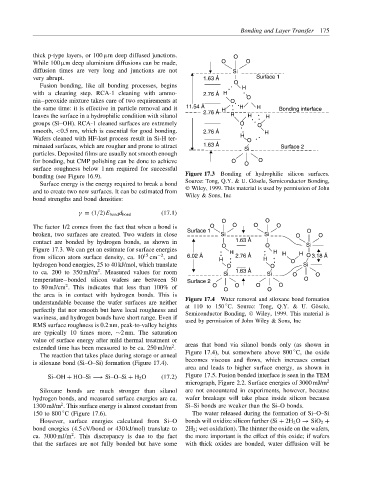
very abrupt. 1.63 Å Surface 1
Fusion bonding, like all bonding processes, begins O H
with a cleaning step. RCA-1 cleaning with ammo- 2.76 Å H
nia–peroxide mixture takes care of two requirements at O O
the same time: it is effective in particle removal and it 11.54 Å 2.76 Å H H H Bonding interface
leaves the surface in a hydrophilic condition with silanol H H H
groups (Si–OH). RCA-1 cleaned surfaces are extremely O O
smooth, <0.5 nm, which is essential for good bonding. 2.76 Å H
Wafers cleaned with HF-last process result in Si-H ter- H O
minated surfaces, which are rougher and prone to attract 1.63 Å Si Surface 2
particles. Deposited films are usually not smooth enough
for bonding, but CMP polishing can be done to achieve O O O
surface roughness below 1 nm required for successful
bonding (see Figure 16.9). Figure 17.3 Bonding of hydrophilic silicon surfaces.
Surface energy is the energy required to break a bond Source: Tong, Q.Y. & U. G¨ osele, Semiconductor Bonding,
and to create two new surfaces. It can be estimated from Wiley, 1999. This material is used by permission of John
Wiley & Sons, Inc
bond strengths and bond densities:
γ = (1/2)E bond d bond (17.1)
O O
The factor 1/2 comes from the fact that when a bond is Surface 1 O O O O O
broken, two surfaces are created. Two wafers in close Si Si O O
contact are bonded by hydrogen bonds, as shown in O 1.63 Å O Si
Figure 17.3. We can get an estimate for surface energies H H H H
15
−2
from silicon atom surface density, ca. 10 cm , and 6.02 Å H 2.76 Å H O O 3.18 Å
hydrogen bond energies, 25 to 40 kJ/mol, which translate O O Si
2
to ca. 200 to 350 mJ/m . Measured values for room Si 1.63 Å Si O O
temperature–bonded silicon wafers are between 50 Surface 2 O
2
to 80 mJ/cm . This indicates that less than 100% of O O O O O O
the area is in contact with hydrogen bonds. This is
understandable because the wafer surfaces are neither Figure 17.4 Water removal and siloxane bond formation
◦
at 110 to 150 C. Source: Tong, Q.Y. & U. G¨ osele,
perfectly flat nor smooth but have local roughness and Semiconductor Bonding, Wiley, 1999. This material is
waviness, and hydrogen bonds have short range. Even if used by permission of John Wiley & Sons, Inc
RMS surface roughness is 0.2 nm, peak-to-valley heights
are typically 10 times more, ∼2 nm. The saturation
value of surface energy after mild thermal treatment or
2
extended time has been measured to be ca. 250 mJ/m . areas that bond via silanol bonds only (as shown in
Figure 17.4), but somewhere above 800 C, the oxide
◦
The reaction that takes place during storage or anneal
becomes viscous and flows, which increases contact
is siloxane bond (Si–O–Si) formation (Figure 17.4).
area and leads to higher surface energy, as shown in
Si–OH + HO–Si −→ Si–O–Si + H 2 O (17.2) Figure 17.5. Fusion bonded interface is seen in the TEM
micrograph, Figure 2.2. Surface energies of 3000 mJ/m 2
Siloxane bonds are much stronger than silanol are not encountered in experiments, however, because
hydrogen bonds, and measured surface energies are ca. wafer breakage will take place inside silicon because
2
1300 mJ/m . This surface energy is almost constant from Si–Si bonds are weaker than the Si–O bonds.
◦
150 to 800 C (Figure 17.6). The water released during the formation of Si–O–Si
However, surface energies calculated from Si–O bonds will oxidize silicon further (Si + 2H 2 O → SiO 2 +
bond energies (4.5 eV/bond or 430 kJ/mol) translate to 2H 2 ; wet oxidation). The thinner the oxide on the wafers,
2
ca. 3000 mJ/m . This discrepancy is due to the fact the more important is the effect of this oxide; if wafers
that the surfaces are not fully bonded but have some with thick oxides are bonded, water diffusion will be