
Page 194 - Sami Franssila Introduction to Microfabrication
P. 194
17
Bonding and Layer Transfer
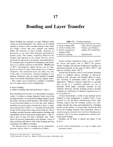
Wafer bonding has emerged in many different appli- Table 17.1 Bonding techniques
cations in microfabrication: two wafers can be bonded
together to create a more versatile starting wafer; bond- • Fusion bonding (FB) Si/Si, SiO 2 /Si, glass/glass
ing creates cavities and seals channels and enables • Anodic bonding (AB) Si/glass, glass/Si/glass
highly 3D structures. In layer transfer, structures are • Thermo-compression Si/glass frit; metal/metal
bonding (TCB)
processed on one wafer, then detached and bonded to • Adhesive bonding Si/polymer/Si
another wafer. This enables completely different tech-
nologies and materials to be merged. Devices can be
processed on silicon for convenience, and transferred to,
◦
Fusion bonding temperature range is up to 1200 C
for example, glass or quartz for transparency and insula-
for silicon and quartz, and ca. 600 C for glasses.
◦
tion, or to a plastic substrate for flexibility. MEMS parts
Anodic bonding and thermo-compression bonding are
or III-V semiconductor optical devices can be trans-
◦
performed typically in the range of 300 to 500 C, and
ferred on silicon IC wafers that contain drive or readout adhesive bonding, below 200 C.
◦
electronics. The transferred layers are often very thin, Similar and dissimilar wafers can be bonded. Bonding
of the order of micrometres, and their handling is very silicon to oxidized silicon, resulting in silicon-on-
delicate. Therefore, they are usually bonded to another insulator, SOI, structure, and bonding silicon to glass,
wafer even before detachment from the original wafer. also resulting in permanent bond, are two typical
Two wafers can be joined by a number of methods, applications. Whereas epitaxial deposition is possible
but two main classes can be distinguished:
only on top of a crystalline substrate, we can, in
principle, bond single crystalline material on any
• direct bonding
• indirect bonding with deposited layers (‘glue’). substrate. However, because bonding involves elevated
temperatures, differences in thermal expansion have to
Direct bonding involves bare or oxidized silicon and glass be accounted for.
wafers. It results in strong chemical bonds across the At least theoretically, a wafer of any material can be
bonding interface, so strong that breakage happens inside bonded at room temperature to another wafer of any
the wafers, and not at bond interface. The bonded wafers material via van der Waals intermolecular forces. This
can be processed further as if it were one wafer. Indirect bonding requires that the bonding surfaces are suffi-
bondingusesagreatvarietyofmaterialsas‘glues’:metals, ciently smooth, flat, clean and terminated by a bonding
glass and polymers (Table 17.1). Bonding methods differ species on the surface. A strong bond can then develop
mostly in their temperature range and permanency. Direct across the bonding interface upon annealing. There is
bonding is usually hermetic and permanent. Bonding with constant progress towards lower and lower bonding tem-
intermediate layers is done at low temperatures, <400 C, peratures, that is, for lower temperatures without sacri-
◦
and it may or may not form a hermetic seal. ‘Glue’ ficing bond strength.
limits the process temperatures and ambients. Some of Bonding can be done at almost any phase of the
these methods applicable to both wafer bonding and chip process:
attachment, like adhesive bonding.
The driving force for bonding can be temperature, • at the wafer manufacturer, as a way to make more
pressure, electric field or a combination of these. advanced wafers;
Introduction to Microfabrication Sami Franssila
2004 John Wiley & Sons, Ltd ISBNs: 0-470-85105-8 (HB); 0-470-85106-6 (PB)