
Page 190 - Sami Franssila Introduction to Microfabrication
P. 190
CMP: Chemical–Mechanical Polishing 169
modification of the oxide: leaching of oxide by the slurry R
softens the top layer, and the mechanical abrasion rate
goes up.
CMP slurries etch without mechanical polishing, just t 2 q h
like fluorine etches silicon without plasma; but in both
etching and CMP, it is the interaction between different t 1
processes that leads to the desired total process: slurry
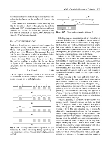
etch rates of 10 nm/min are typical, but CMP removal Figure 16.7 Planarization relaxation distance R
rates of 500 nm/min are standard.
Polishing rate and planarization rate are two different
concepts. Polishing rate is applicable to one material.
16.4 APPLICATIONS OF CMP
Planarization rate is the rate of decrease in step height:
Conformal deposition processes replicate the underlying the high peaks are polished, which decreases step height,
topography dutifully. Such processes are useful in gap but some material is removed from the valleys too,
filling: small spaces between lines are completely filled which decreases the planarization rate. Towards the end
without any voids. However, this argument does not of the process, the planarization rate drops to zero, even
hold for larger linewidths: step height is unchanged after though the overall polishing rate is still finite.
conformal deposition, as shown in Figure 16.6(a). Selectivity in CMP bears close resemblance to
Some deposited CVD films flow, or have flow- etching: we need to know the polish rates of the top and
like profiles, resulting in profiles like the one shown bottom films in order to calculate, for instance, substrate
in Figure 16.6(b). Spin-on dielectrics flow over the loss during overpolishing. Identically to etching, it is
topography, but the planarization length (Figure 16.7) sometimes beneficial to have the same 1:1 selectivity
defined as between films, but, most often, it is desirable to remove
R = h/ tan θ (16.4) one film relatively rapidly, and to have high selectivity
against the bottom film, which can then be processed in
is in the range of micrometres or tens of micrometres in a separate step.
the maximum, as shown in Figure 16.6(c). CMP is the Oxide polishing is the oldest and most widely prac-
closest you can get to global planarity. ticed CMP process. Its main application is planarization
in multi-level metallization in advanced ICs, where it
provides a planar surface that makes subsequent lithog-
raphy and deposition steps easy. One problem with oxide
polishing is the lack of endpoint: there is no clear end for
polishing. This is called blind polishing. The opposite is
(a)
stopped polishing, in which, for instance, a nitride layer
acts as a polish stop (cf. etch-stop layer) but selectivities
are not necessarily very high.
Tungsten polishing is another CMP process that was
adopted rapidly. Contact holes and via holes are filled
(b)
by CVD tungsten, which is then removed from planar
areas, leaving just the contact plug filled with metal
(Figure 16.1(c)). The same structure can, of course, be
obtained by tungsten etchback, and the first implemen-
tations of tungsten plug process did use etchback. CMP
(c)
has proven to be better with respect to plug loss: at etch-
ing end point, the etchable area decreases dramatically
and the etchant will attack the tungsten in the plug, lead-
ing to severe plug recess. CMP is much better in this
(d) respect, but, naturally, process optimization with either
Figure 16.6 Planarity: (a) conformal deposition, no pla- technology can bring about improvements.
narization; (b) surface smoothing during deposition; (c) CMP is used whenever global planarity is required. In
local planarization by spin-film and (d) global planarization addition to multi-level metallization for ICs, other appli-
by CMP cations have sprung up. In superconducting quantum