Page 185 - Sami Franssila Introduction to Microfabrication
P. 185
164 Introduction to Microfabrication


              Implant dose is monitored during implantation by the  annealing. Its dislocation densities can be a million/cm ,
                                                                                                 2
            Faraday cup current measurement. This is the basis for  orders of magnitude more than in bulk silicon. Implan-
            the high degree of doping control in implantation as  tation time poses another limitation: the required doses
            compared to diffusion, which has no, whatsoever, in situ  are two orders of magnitude higher than those in com-
                                                                                              17
            monitoring method.                           mon usage. A low dose SIMOX with 4 × 10 /cm 2
                                                         implantation helps to minimize both the aforementioned
                                                         problems. There are further limitations that are inherent
            15.4.2 Safety aspects
                                                         to the implant process: with 200 keV maximum energy,
            Ion implanters pose a number of safety issues that have  the implant depth is fairly shallow and, therefore, the
            to be tackled. The obvious one is the high voltage  device silicon thickness is rather limited. The thickness
            that is present inside the machines. The second issue  of buried is also limited by the implant process.
            is X-rays that are produced as ions decelerate. Lead
            radiation protection is routinely used around the parts
            where X-rays are generated. If hydrogen is implanted, as  15.6 EXERCISES
            in the Smart-cut process (to be presented in Chapter 17),
            nuclear reactions are possible at fairly low energies of  1. What will be the implant time for a 200 mm
            150 keV and gamma rays are then generated.      diameter wafer, when arsenic ions are implanted
                                                                          15
                                                                              2
              Implant gases AsH 3 , PH 3 and BF 3 are extremely  with doses of 10 /cm  and implant current of
            toxic. Toxic gas detectors are placed inside the system  100 µA?     11  +  49   +
            to sniff for leaks. Operation and maintenance of an  2. What is the range of 20 keV  B and  BF 2  ions?
            implanter can, therefore, be carried out by highly trained  3. How thick a silicon dioxide layer will be formed
            staff only. More discussions on safety issues can be  inside the silicon when the implant dose is 2 ×
                                                              18
                                                                  2
            found in connection with cleanrooms, in Chapter 35.  10 /cm in SIMOX?
                                                          4. What is the range of 100 keV germanium implanta-
                                                            tion?
            15.5 SIMOX: SOI BY ION IMPLANTATION          5S. How thick an oxide layer is needed to mask boron
                                                            implantation? Present your results as a function of
            In SIMOX technology, a SOI structure is realized in two
                                                            boron energy.
            main steps. The first step is oxygen implantation into a
                                                         6S. Check by simulator the range of 100 keV phospho-
            silicon wafer and the second step is a high-temperature  rus ions and compare it with the simple estimate
            anneal during which the implanted oxygen atoms form  discussed in the text.
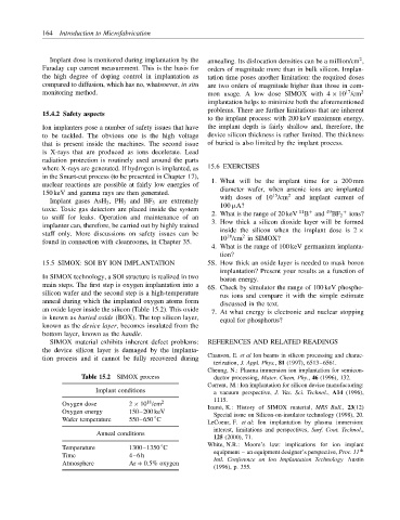
            an oxide layer inside the silicon (Table 15.2). This oxide  7. At what energy is electronic and nuclear stopping
            is known as buried oxide (BOX). The top silicon layer,  equal for phosphorus?
            known as the device layer, becomes insulated from the
            bottom layer, known as the handle.
              SIMOX material exhibits inherent defect problems:  REFERENCES AND RELATED READINGS
            the device silicon layer is damaged by the implanta-
            tion process and it cannot be fully recovered during  Chanson, E. et al Ion beams in silicon processing and charac-
                                                          terization, J. Appl. Phys., 81 (1997), 6513–6561.
                                                         Cheung, N.: Plasma immersion ion implantation for semicon-
                       Table 15.2 SIMOX process           ductor processing, Mater. Chem. Phy., 46 (1996), 132.
                                                         Current, M.: Ion implantation for silicon device manufacturing:
                           Implant conditions             a vacuum perspective, J. Vac. Sci. Technol., A14 (1996),
                                                          1115.
                                        18
                  Oxygen dose       2 × 10 /cm 2         Izumi, K.: History of SIMOX material, MRS Bull., 23(12)
                  Oxygen energy     150–200 keV           Special issue on Silicon-on-insulator technology (1998), 20.
                                          ◦
                  Wafer temperature  550–650 C
                                                         LeCoeur, F. et al: Ion implantation by plasma immersion:
                                                          interest, limitations and perspectives, Surf. Coat. Technol.,
                           Anneal conditions
                                                          125 (2000), 71.
                                                         White, N.R.: Moore’s law: implications for ion implant
                  Temperature       1300–1350 C                                                  th
                                            ◦
                  Time              4–6 h                 equipment – an equipment designer’s perspective, Proc. 11
                                                          Intl. Conference on Ion Implantation Technology Austin
                  Atmosphere        Ar + 0.5% oxygen
                                                          (1996), p. 355.

