
Page 181 - Sami Franssila Introduction to Microfabrication
P. 181
160 Introduction to Microfabrication
Target surface Table 15.1 Energy loss of implanted ions in silicon
Nuclear stopping in silicon (independent of energy) in
keV/µm
Incident ion beam R L
Boron 92
R R P Phosphorus 447
Arsenic 1160
RL
Electronic stopping in silicon in keV/µm
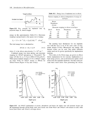
Figure 15.2 Key concepts for implanted ions: R p
projected range, R L lateral straggle E/keV Boron Phosphorus Arsenic
10 65 88 90
50 145 196 200
energy in this approximation (Table 15.1). Electronic 100 205 277 283
stopping is proportional to the square root of energy: 200 290 391 401
S e = 3.3 × 10 −17 (Z 1 + Z 2 )(E/M 1 ) 1/2 eVcm 2
(15.2)
The total energy loss is calculated as The masking layer thicknesses for ion implanta-
tion will thus have to be of the same order of mag-
dE/dx = −(S n + S e )N (15.3) nitude (Figure 15.3(b)). Photoresists suit ideally, and
thermal oxides can be used. But unlike diffusion,
−3
22
where N is the silicon atom density, 5 × 10 cm . oxides need not be grown specifically for implantation
Combined energy loss from nuclear and electronic masking.
stopping for 100 keV phosphorus is 724 µm/keV. The Thin oxides, in the 10 nm range, are grown on silicon
range will then be ca. 0.14 µm (100 keV/724 µm/keV). before implantation for two reasons: implantation is a
With typical implant energies of 10 to 200 keV ranges high-energy process, and accelerated ions sputter metal
are from 10 nm for 10 keV arsenic to 500 nm for atoms from the implanter hardware. The thin oxide pre-
200 keV boron (Figure 15.3(a) and 15.4(a)). vents these metal atoms from penetrating the silicon.
SiO 2
10 21 10 21
Arsenic Arsenic
Phosphorous Arsenic
Boron 10 20 Boron
20
10
Boron
Concentration (cm −3 ) 10 19 Concentration (cm −3 ) 10 19
18
18
10
10
10
16
16
10 17 10 17
10
10 15 10 15
0.00 0.20 0.40 0.60 0.80 1.00 0.00 0.20 0.40 0.60 0.80 1.00
Depth (µm) Depth (µm)
(a) (b)
Figure 15.3 (a) 100 keV implantation of arsenic, phosphorus and boron: the lighter ions will penetrate deeper and
(b) implantation through 250 nm thick oxide: most arsenic ions (both 50 keV and 150 keV) will remain in oxide, while
boron (both 50 keV and 150 keV) will dope silicon