
Page 178 - Sami Franssila Introduction to Microfabrication
P. 178
Diffusion 157
10 18 13:22:24 24-JAN-:3 10 21 12:36:20 24-JAN-:3
Boron Boron
Phosphors Phosphors
Phosphors
10 17 Phosphors 10 20 oxthi = 0.1000 Phosphors
Phosphors
10 19
Concentration (cm −3 ) 10 15 Concentration (cm −3 ) 10 18
16
10
17
10
14
10
10 16
10 13 15
10
10 14
10 12 0.50 1.00 1.50 2.00 2.50 3.00 0.00 0.20 0.40 0.60 0.80 1.00
0.00
Depth in µm Depth in µm
(a) (b)
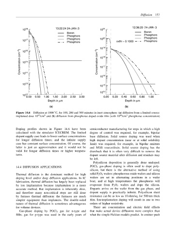
Figure 14.6 Diffusion at 1000 C, for 100, 200 and 300 minutes in inert atmosphere: (a) diffusion from a limited source:
◦
13
2
20
3
implanted dose 10 /cm and (b) diffusion from phosphorus doped oxide film (with 10 /cm phosphorus concentration)
Doping profiles shown in Figure 14.6 have been semiconductor manufacturing for steps in which a high
calculated with the simulator ICECREM. The limited degree of control was required, for example, bipolar
dopant supply case leads to lower surface concentrations base diffusion. Solid source doping was used when
for longer diffusion times; and the infinite supply high dopant concentration (near or at solid solubility
case has constant surface concentration. Of course, the limit) was required, for example, in bipolar emitters
latter is just an approximation and it would not be and MOS source/drain. Solid source doping has the
valid for longer diffusion times or higher tempera- drawback that it is often very difficult to remove the
tures. dopant source material after diffusion and residues may
be left.
Polysilicon deposition is generally done undoped.
14.4 DIFFUSION APPLICATIONS POCl 3 gas-phase doping is often used to dope poly-
silicon, but there is the alternative method of using
Thermal diffusion is the dominant method for high solid P 2 O 5 wafers: phosphorous oxide wafers and silicon
doping level and/or deep diffusion applications. In IC wafers are set in alternating positions in a wafer
fabrication, thermal diffusion has largely been replaced boat, and at high temperatures the phosphorus will
by ion implantation because implantation is a more evaporate from P 2 O 5 wafers and dope the silicon.
accurate method. But implantation is inherently slow, Dopants arrive on the wafer from the gas phase, and
and therefore many non-critical steps are still done dopant supply is practically infinite. Polysilicon sheet
by furnace thermal diffusion: the furnaces are much resistance can be as low as 10 ohm/sq, for 500 nm thick
simpler equipment than implanters. The double-sided film. Ion-implantation doping will result in one to two
nature of thermal diffusion is sometimes advantageous orders of higher resistivity.
for volume devices. There are concentration and electric field effects
Gas-phase doping by POCl 3 gas for n-type and that make actual device diffusions more complex than
BBr 3 gas for p-type was used in the early years of what the simple Fickian models predict. In emitter-push