
Page 174 - Sami Franssila Introduction to Microfabrication
P. 174
14
Diffusion
The power of silicon technology stems from the ability • during crystal growth
to tailor dopant concentrations over eight orders of • by neutron transmutation doping (NTD)
magnitude by introducing suitable n- or p-type dopants • during epitaxy
into the silicon. The upper limit is set by solid solubility • by ion implantation
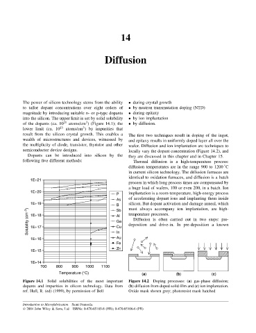
3
of the dopants (ca. 10 21 atoms/cm ) (Figure 14.1); the • by diffusion.
3
lower limit (ca. 10 13 atoms/cm ) by impurities that
result from the silicon crystal growth. This enables a The first two techniques result in doping of the ingot,
wealth of microstructures and devices, witnessed by and epitaxy results in uniformly doped layer all over the
the multiplicity of diode, transistor, thyristor and other wafer. Diffusion and ion implantation are techniques to
semiconductor device designs. locally vary the dopant concentration (Figure 14.2), and
Dopants can be introduced into silicon by the they are discussed in this chapter and in Chapter 15.
following five different methods: Thermal diffusion is a high-temperature process:
diffusion temperatures are in the range 900 to 1200 C
◦
in current silicon technology. The diffusion furnaces are
identical to oxidation furnaces, and diffusion is a batch
1E+21
process in which long process times are compensated by
a huge load of wafers, 100 or even 200, in a batch. Ion
1E+20
P implantation is a room-temperature, high-energy process
As of accelerating dopant ions and implanting them inside
1E+19 B silicon. But dopant activation and damage anneal, which
must always accompany ion implantation, are high-
Sb
Solubility (cm −3 ) 1E+18 Al temperature processes.
Diffusion is often carried out in two steps: pre-
Ga
deposition and drive-in. In pre-deposition a known
Cu
1E+17
Au
1E+16 In
Fe
Zn
1E+15
1E+14
700 800 900 1000 1100
Temperature (°C) (a) (b) (c)
Figure 14.1 Solid solubilities of the most important Figure 14.2 Doping processes: (a) gas-phase diffusion;
dopants and impurities in silicon technology. Data from (b) diffusion from doped solid film and (c) ion implantation.
ref. Hull, R. (ed) (1999), by permission of Bell Oxide mask shown grey; photoresist mask hatched
Introduction to Microfabrication Sami Franssila
2004 John Wiley & Sons, Ltd ISBNs: 0-470-85105-8 (HB); 0-470-85106-6 (PB)