
Page 175 - Sami Franssila Introduction to Microfabrication
P. 175
154 Introduction to Microfabrication
and limited number of dopants is introduced on the −3
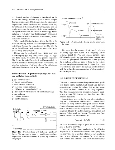
Dopant concentration (cm )
wafer, and during drive-in they will diffuse deeper.
Ion implantation and diffusion are strongly interrelated: p anode
+
implantation can be considered as a pre-deposition step 1 × 10 20 epi Substrate wafer
+
for diffusion. Diffusion is, therefore, the general term for n cathode
doping processes, irrespective of the actual mechanism p-base +
of dopant introduction. In silicon IC technology dopant n buried layer
diffusion is such a key step that the country of origin of
semiconductor devices is defined as the country where 1 × 10 15 n-collector Depth into
diffusions were made. silicon
When local diffusion is done, silicon dioxide is the Figure 14.4 UV-photodiode doping profile underneath
standard masking material. Even though the dopants do the anode
not diffuse through the oxide, they do modify it to the
extent that diffusion mask oxides are practically always
etched away after diffusion. The area directly underneath the anode changes
Doping can be performed many times over, and its doping type three times: it is originally n-type
silicon doping type may change from p-type to n-type epilayer, doped by PH 3 gas during epitaxy. Base
and back again, depending on the process sequence. diffusion changes it to p-type when boron concentration
The device shown in Figure 14.3, an UV-photodiode, is exceeds the phosphorus concentration in the epilayer;
made in a modified npn-bipolar process. UV-photons are the n-cathode diffusion turns it back to the n-type
+
absorbed in the top p diffusion layer. We will discuss because phosphorus concentration is higher than boron
only the diffusion aspects of the device now. concentration; and finally, the surface anode diffusion
with the highest boron concentration of all results in p +
silicon (Figure 14.4).
Process flow for UV-photodiode (lithography, etch
and oxidation steps omitted)
14.1 DIFFUSION MECHANISMS
p-type substrate wafer
+
n buried layer diffusion Diffusion is atom movement along concentration gradi-
n epitaxial layer deposition ents. Fairly simple mathematical models can describe
+
p substrate contact diffusion concentration profiles in solids, but at the atom-
+
n diffusion to contact buried layer istic level diffusion remains to be fully explained.
+
p base contact enhancement diffusion (under A IR ) This has consequences for simulators, because mech-
p base diffusion anisms are not fully known, and therefore, modelling
+
n cathode diffusion remains inaccurate.
+
p anode diffusion. Dopant atoms move with the help of point defects:
they jump to vacancies and interstitials. Substitutional
dopants are fairly stable without point defects. Vacan-
UV-photodiode cies are always present through thermal equilibrium pro-
Substrate cesses: vacancies are thermodynamic defects, and their
contact A IR Cathode Anode nature is different from, for example, dislocations and
P + stacking faults, which are ‘frozen’. Vacancies as a frac-
P + P N + tion of all sites can be estimated by
P + N +
N f = exp(−E a /kT ) (14.1)
N +
For 1 eV activation energy, it gives ca. 0.01% vacant
sites at 1000 C (1273 K).
◦
P substrate
Here, we outline some mechanisms for diffusion
Figure 14.3 UV-photodiode with shallow p+ anode dif- (Figure 14.5). In interstitial diffusion, atoms jump from
fusion. The structure is based on npn-bipolar transistor. one interstitial site to another, which is always available.
Reproduced from Zimmermann, H. (1999), by permission This is the diffusion mechanism for small atoms,
of Springer like sodium and lithium. The substitutional/vacancy