
Page 180 - Sami Franssila Introduction to Microfabrication
P. 180
15
Ion Implantation
Ion implantation is a process in which accelerated it is one-third of the vertical range, whereas diffusion is
ions hit the silicon wafer, penetrate into the silicon, an isotropic process in the first approximation.
slow down by collisional and stochastic processes and Implantation is a room-temperature process in theory.
come to rest within femtoseconds at the top micrometre Photoresist masking is enough, which makes implan-
layer. One application, introduction of dopants (As, tation easier than thermal diffusion, but implantation
P, B) into silicon, is by far the most important is always connected with a high temperature anneal
one, but implantation offers many possibilities. Heavy step because introduction of dopants is not enough; the
ions can modify materials by introducing damage and dopants have to be activated, that is, they have to find the
amorphization, which can sometimes be beneficial, even lattice sites. Implantation also damages the silicon crys-
though damage in general is considered to be a drawback tal, and in order to recover defect-free single-crystalline
of implantation. Implantation of oxygen inside silicon, state, this damage has to be annealed away. Activation
and subsequent silicon dioxide formation, is used to of dopants and damage removal can sometimes be one
make SOI wafers. and the same anneal, but as will be discussed in the
Ion implantation can be used to produce a great Chapter 25, this is not always straightforward.
variety of doping profiles inside silicon. Maximum
dopant density need not be at the wafer surface; it can 15.1 THE IMPLANT PROCESS
be at hundreds of nanometres deep inside the silicon
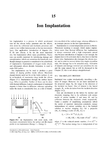
(Figure 15.1). Implantation through the surface layers Implanted ions scatter stochastically, travelling a dis-
(e.g., SiO 2 ) is possible. Neither of these can be done tance R (range). However, we are more interested in
with thermal diffusion. Lateral confinement of implanted the projected range, R p , the range in the direction of
dopants is better than in diffusion: sideways spreading the incident ion beam. Also of interest is the lateral
under the mask is considerably less, as a rule of thumb, straggle, R L , or the deviation from the incident direction
(Figure 15.2).
Ions are decelerated in the lattice by nuclear and
electronic stopping, that is, by collisions with atomic
nuclei of atomic number Z and mass M, and by
collisions between the electronic cloud, respectively.
Concentration E1 the nature of material, interaction potentials, energy
Under a number of simplifying assumptions (about
independence of various variables, etc.,), the Linhard
E2
(M 1 , Z 1 ) hitting a wafer of (M 2 , Z 2 ) is
C subs solution to nuclear stopping (S n ) for a projectile
Depth S n = 2.8 × 10 −15 (Z 1 Z 2 /Z)
(a) (b) × (M 1 /(M 1 + M 2 )) unit: eVcm 2 (15.1)
Figure 15.1 (a) Implantation with resist mask, with 2/3
maximum concentration below the surface and (b) dopant where Z is the reduced atomic number, Z = (Z 1 +
)
profile in ion implantation (Energy 1 > Energy 2) Z 2/3 1/2 . The nuclear energy loss is independent of ion
2
Introduction to Microfabrication Sami Franssila
2004 John Wiley & Sons, Ltd ISBNs: 0-470-85105-8 (HB); 0-470-85106-6 (PB)