
Page 179 - Sami Franssila Introduction to Microfabrication
P. 179
158 Introduction to Microfabrication
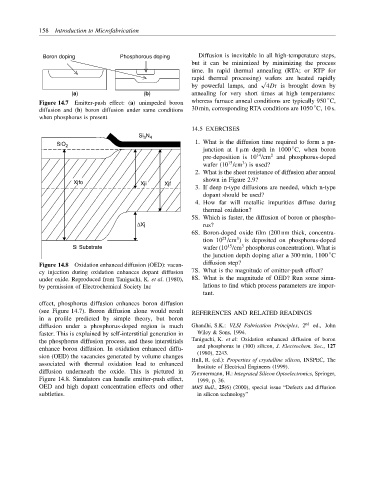
Boron doping Phosphorous doping Diffusion is inevitable in all high-temperature steps,
but it can be minimized by minimizing the process
time. In rapid thermal annealing (RTA; or RTP for
rapid thermal processing) wafers are heated rapidly
√
by powerful lamps, and 4Dt is brought down by
(a) (b) annealing for very short times at high temperatures:
◦
Figure 14.7 Emitter-push effect: (a) unimpeded boron whereas furnace anneal conditions are typically 950 C,
◦
diffusion and (b) boron diffusion under same conditions 30 min, corresponding RTA conditions are 1050 C, 10 s.
when phosphorus is present
14.5 EXERCISES
Si 3 N 4
1. What is the diffusion time required to form a pn-
SiO 2
◦
junction at 1 µm depth in 1000 C, when boron
14
2
pre-deposition is 10 /cm and phosphorus-doped
15
3
wafer (10 /cm ) is used?
2. What is the sheet resistance of diffusion after anneal
Xjfo Xji Xjf shown in Figure 2.9?
3. If deep n-type diffusions are needed, which n-type
dopant should be used?
4. How far will metallic impurities diffuse during
thermal oxidation?
5S. Which is faster, the diffusion of boron or phospho-
∆Xj rus?
6S. Boron-doped oxide film (200 nm thick, concentra-
3
21
tion 10 /cm ) is deposited on phosphorus-doped
15
Si Substrate wafer (10 /cm phosphorus concentration). What is
3
the junction depth doping after a 300 min, 1100 C
◦
diffusion step?
Figure 14.8 Oxidation enhanced diffusion (OED): vacan-
cy injection during oxidation enhances dopant diffusion 7S. What is the magnitude of emitter-push effect?
under oxide. Reproduced from Taniguchi, K. et al. (1980), 8S. What is the magnitude of OED? Run some simu-
by permission of Electrochemical Society Inc lations to find which process parameters are impor-
tant.
effect, phosphorus diffusion enhances boron diffusion
(see Figure 14.7). Boron diffusion alone would result REFERENCES AND RELATED READINGS
in a profile predicted by simple theory, but boron
diffusion under a phosphorus-doped region is much Ghandhi, S.K.: VLSI Fabrication Principles, 2 nd ed., John
faster. This is explained by self-interstitial generation in Wiley & Sons, 1994.
the phosphorus diffusion process, and these interstitials Taniguchi, K. et al: Oxidation enhanced diffusion of boron
enhance boron diffusion. In oxidation enhanced diffu- and phosphorus in (100) silicon, J. Electrochem. Soc., 127
(1980), 2243.
sion (OED) the vacancies generated by volume changes Hull, R. (ed.): Properties of crystalline silicon, INSPEC, The
associated with thermal oxidation lead to enhanced Institute of Electrical Engineers (1999).
diffusion underneath the oxide. This is pictured in Zimmermann, H.: Integrated Silicon Optoelectronics, Springer,
Figure 14.8. Simulators can handle emitter-push effect, 1999, p. 36.
OED and high dopant concentration effects and other MRS Bull., 25(6) (2000), special issue “Defects and diffusion
subtleties. in silicon technology”