
Page 182 - Sami Franssila Introduction to Microfabrication
P. 182
Ion Implantation 161
In the post implantation clean, this thin pad oxide and interface. These are known as end-of-range (EOR)
the metals on it can easily be removed by a HF dip. defects. If the concentration of dopants is above solid
Thin oxides serve also to randomize incoming ions, solubility limit, dopants precipitate.
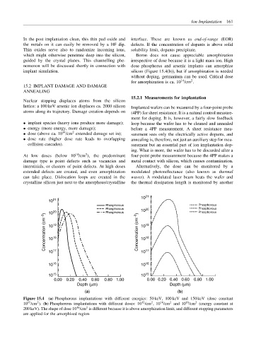
which might otherwise penetrate deep into the silicon, Boron does not cause appreciable amorphization
guided by the crystal planes. This channelling phe- irrespective of dose because it is a light mass ion. High
nomenon will be discussed shortly in connection with dose phosphorus and arsenic implants can amorphize
implant simulation. silicon (Figure 15.4(b)), but if amorphization is needed
without doping, germanium can be used. Critical dose
2
14
for amorphization is ca. 10 /cm .
15.2 IMPLANT DAMAGE AND DAMAGE
ANNEALING
15.2.1 Measurements for implantation
Nuclear stopping displaces atoms from the silicon
lattice: a 100 keV arsenic ion displaces ca. 2000 silicon Implanted wafers can be measured by a four-point probe
atoms along its trajectory. Damage creation depends on (4PP) for sheet resistance. It is a natural control measure-
ment for doping. It is, however, a fairly slow feedback
• implant species (heavy ions produce more damage); loop because the wafer has to be cleaned and annealed
• energy (more energy, more damage); before a 4PP measurement. A sheet resistance mea-
14
2
• dose (above ca. 10 /cm extended damage set in); surement sees only the electrically active dopants, and
• dose rate (higher dose rate leads to overlapping annealing is, therefore, not just an auxiliary step for mea-
collision cascades). surement but an essential part of ion implantation dop-
ing. What is more, the wafer has to be discarded after a
2
14
At low doses (below 10 /cm ), the predominant four-point probe measurement because the 4PP makes a
damage type is point defects such as vacancies and metal contact with silicon, which causes contamination.
interstitials, or clusters of point defects. At high doses Alternatively, the dose can be monitored by a
extended defects are created, and even amorphization modulated photoreflectance (also known as thermal
can take place. Dislocation loops are created in the waves). A modulated laser beam heats the wafer and
crystalline silicon just next to the amorphous/crystalline the thermal dissipation length is monitored by another
10 21
10 21
Phosphorous Phosphorous
Phosphorous 10 20 Phosphorous
10 20 Phosphorous Phosphorous
Concentration (cm −3 ) 10 19 Concentration (cm −3 ) 10 19
18
18
10
10
10
16
16
10
10 17 10 17
10 15 10 15
0.00 0.20 0.40 0.60 0.80 1.00 0.00 0.20 0.40 0.60 0.80 1.00
Depth (µm) Depth (µm)
(a) (b)
Figure 15.4 (a) Phosphorous implantations with different energies: 50 keV, 100 keV and 150 keV (dose constant
2
14
16
2
15
2
2
12
10 /cm ). (b) Phosphorous implantations with different doses: 10 /cm , 10 /cm and 10 /cm (energy constant at
2
16
200 keV). The shape of dose 10 /cm is different because it is above amorphization limit, and different stopping parameters
are applied for the amorphized region