
Page 183 - Sami Franssila Introduction to Microfabrication
P. 183
162 Introduction to Microfabrication
small power laser. The dissipation lengths are correlated simulator SRIM (Simulation of Ranges of Ions in Mat-
to the implant damage, and therefore to the dose. This ter) is a widely used MC simulator for implantation and
is a fast, non-contact, non-specific measurement, which other ion-beam processes.
needs no wafer preparation, and can be done even on Input for a prototypical semi-analytical implantation
photoresist-patterned wafers. simulation includes:
Point defects created by implantation cannot be
seen by physical analysis, but extended defects like – wafer type and dopant concentration
dislocations can be seen by TEM. Amorphization can – ion specie
be measured by TEM or by XRD. – energy
– dose.
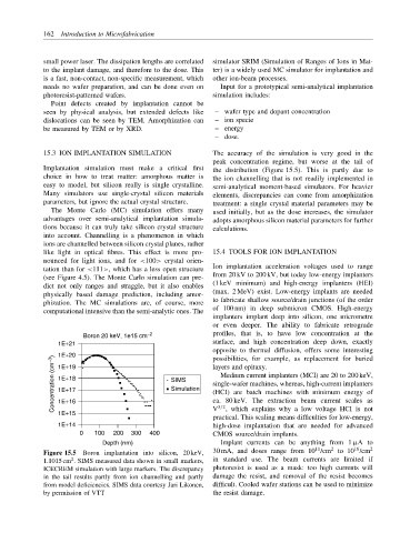
15.3 ION IMPLANTATION SIMULATION The accuracy of the simulation is very good in the
peak concentration regime, but worse at the tail of
Implantation simulation must make a critical first the distribution (Figure 15.5). This is partly due to
choice in how to treat matter: amorphous matter is the ion channelling that is not readily implemented in
easy to model, but silicon really is single crystalline. semi-analytical moment-based simulators. For heavier
Many simulators use single-crystal silicon materials elements, discrepancies can come from amorphization
parameters, but ignore the actual crystal structure. treatment: a single crystal material parameters may be
The Monte Carlo (MC) simulation offers many used initially, but as the dose increases, the simulator
advantages over semi-analytical implantation simula- adopts amorphous silicon material parameters for further
tions because it can truly take silicon crystal structure calculations.
into account. Channelling is a phenomenon in which
ions are channelled between silicon crystal planes, rather
like light in optical fibres. This effect is more pro- 15.4 TOOLS FOR ION IMPLANTATION
nounced for light ions, and for <100> crystal orien-
Ion implantation acceleration voltages used to range
tation than for <111>, which has a less open structure
from 20 kV to 200 kV, but today low-energy implanters
(see Figure 4.5). The Monte Carlo simulation can pre-
(1 keV minimum) and high-energy implanters (HEI)
dict not only ranges and straggle, but it also enables
(max. 2 MeV) exist. Low-energy implants are needed
physically based damage prediction, including amor-
to fabricate shallow source/drain junctions (of the order
phization. The MC simulations are, of course, more
of 100 nm) in deep submicron CMOS. High-energy
computational intensive than the semi-analytic ones. The
implanters implant deep into silicon, one micrometre
or even deeper. The ability to fabricate retrograde
Boron 20 keV, 1e15 cm −2 profiles, that is, to have low concentration at the
1E+21 surface, and high concentration deep down, exactly
opposite to thermal diffusion, offers some interesting
1E+20 possibilities, for example, as replacement for buried
Concentration (cm −3 ) 1E+18 SIMS single-wafer machines, whereas, high-current implanters
1E+19
layers and epitaxy.
Medium current implanters (MCI) are 20 to 200 keV,
Simulation
1E+17
(HCI) are batch machines with minimum energy of
ca. 80 keV. The extraction beam current scales as
1E+16
3/2
, which explains why a low voltage HCI is not
V
1E+15
practical. This scaling means difficulties for low-energy,
1E+14 high-dose implantation that are needed for advanced
0 100 200 300 400 CMOS source/drain implants.
Depth (nm) Implant currents can be anything from 1 µA to
2
11
16
Figure 15.5 Boron implantation into silicon, 20 keV, 30 mA, and doses range from 10 /cm to 10 /cm 2
2
1.1015 cm . SIMS measured data shown in small markers, in standard use. The beam currents are limited if
ICECREM simulation with large markers. The discrepancy photoresist is used as a mask: too high currents will
in the tail results partly from ion channelling and partly damage the resist, and removal of the resist becomes
from model deficiencies. SIMS data courtesy Jari Likonen, difficult. Cooled wafer stations can be used to minimize
by permission of VTT the resist damage.