
Page 171 - Sami Franssila Introduction to Microfabrication
P. 171
150 Introduction to Microfabrication
for thin oxides. Data from Massoud, H.Z. et al: J.
Electrochem. Soc., 132 (1985), 2685.
Si(100)
Time (min) 850 C 1000 C
◦
◦
(a) (d)
20 6 nm 26 nm
SiO 2 40 8 nm 42 nm
60 11 nm 56 nm
80 13 nm 68 nm
(e)
(b) 4S. Phosphorus-doped polysilicon (20–80 ohm/sq) oxi-
dation produces 50 nm thick oxide in 30 min dry
◦
◦
Cr oxidation at 1000 C. At 900 C, dry oxidation
results in 10 nm thick oxide. How do these values
(f) compare with single-crystal silicon oxidation?
5S. High-pressure oxidation (HIPOX) increases oxida-
◦
tion rates. Data for dry oxidation at 900 C is given
below. Data from Lie, L.N. et al: J. Electrochem.
(c) Cr Soc., 129 (1982), 2828.
(g)
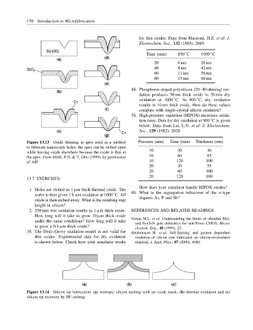
Figure 13.13 Oxide thinning at apex used as a method Pressure (atm) Time (min) Thickness (nm)
to fabricate nanoscopic holes: the apex can be etched open
while leaving oxide elsewhere because the oxide is thin at 10 30 40
the apex. From Minh, P.N. & T. Ono (1999), by permission 10 60 65
of AIP 10 120 100
20 30 55
20 60 100
20 120 180
13.7 EXERCISES
How does your simulator handle HIPOX oxides?
1. Holes are etched in 1 µm thick thermal oxide. The
wafer is then given 1 h wet oxidation at 1000 C. All 6S. What is the segregation behaviour of the n-type
◦
oxide is then etched away. What is the resulting step dopants As, P and Sb?
height in silicon?
2. 250 min wet oxidation results in 1 µm thick oxide. REFERENCES AND RELATED READINGS
How long will it take to grow 10 µm thick oxide
Green, M.L. et al: Understanding the limits of ultrathin SiO 2
under the same conditions? How long will it take
and Si–O–N gate dielectrics for sub-50 nm CMOS, Micro-
to grow a 0.1 µm thick oxide?
electron. Eng., 48 (1999), 25.
3S. The Deal–Grove oxidation model is not valid for Heidemayer, H. et al: Self-limiting and pattern dependent
thin oxides. Experimental data for dry oxidation oxidation of silicon dots fabricated on silicon-on-insulator
is shown below. Check how your simulator works material, J. Appl. Phys., 87 (2000), 4580.
(a) (b) (c)
Figure 13.14 Silicon tip fabrication: (a) isotropic silicon etching with an oxide mask; (b) thermal oxidation and (c)
silicon tip recovery by HF etching