
Page 167 - Sami Franssila Introduction to Microfabrication
P. 167
146 Introduction to Microfabrication
Oxygen atom
Silicon atom
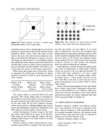
Figure 13.5 Basic structure of silica: a silicon atom Figure 13.6 The structure of silicon–silicon dioxide
tetrahedrally bonds to four oxygen atoms interface: some silicon atoms have dangling bonds
interstitial positions. Boron and phosphorus can take the the film and anneals out some defects. It of course
position of a silicon atom in the network and form oxides adds to thermal load, and has to be considered when
themselves (B 2 O 3 , P 2 O 5 ), hence the name network doping profiles are fine-tuned. Hydrogen anneal is often
formers. However, due to their electrical properties, they used to passivate dangling bonds: hydrogen attaches to
affect oxide differently. Phosphorus, a group V element, the free valence of the silicon, and eliminates further
will donate an extra electron to a non-bridging oxygen charge trapping. However, high electric fields can easily
and stabilize the oxide, whereas boron with one electron accelerate electrons to such energies that hydrogen
missing makes oxide less stable. Sodium, potassium and atoms are released during device operation.
lead are interstitial network modifiers that bond to one Oxide thickness is usually measured by optical meth-
silicon atom only and do not form glasses themselves. ods: either by ellipsometry or reflectometry. Thermal
When silicon and oxygen react to form SiO 2 , silicon oxides can be grown with very tight specifications, for
is consumed: for an SiO 2 layer of thickness D, silicon a 10 nm thick oxide, uniformity is 1%, that is, equal
thickness consumed is 0.45D as can be calculated from to one atomic diameter. For thermal oxides, refrac-
molar volumes: tive index value n = 1.46 is usually used, but for very
thin oxides this is not valid. A quick and easy way to
gauge oxide thickness is by its colour; Table 5.7 shows
Density of Si Molar mass Molar volume
3
2.3 g/cm 3 28 g/mol 12.17 cm /mol oxide colours.
Density of SiO 2 Molar mass Molar volume Various electrical measurements are also used: break-
3
2.2 g/cm 3 60 g/mol 27.27 cm /mol down voltage is one of many. High-quality silicon diox-
ide can sustain 10 MV/cm, even 12 MV/cm, while poly-
oxides have 5 MV/cm breakdown fields. Oxide defects
The original surface is somewhat below the oxide and electrical quality are closely connected; this topic
mid-point. This volume change leads to restrictions in will be discussed further in Chapter 24.
the oxidation of structured surfaces, because stresses can
become excessively large in the corners of the structures.
13.4 SIMULATION OF OXIDATION
On the other hand, the fact that oxidation consumes
silicon can be used as a cleaning method: thin oxide is Oxidation simulation, together with diffusion simula-
grown and immediately removed by hydrofluoric acid tion, is the backbone of all process integration simu-
(HF) etching, to reveal a perfect silicon surface. lators. Thermal oxidation is well understood, and can
Another consequence of volume change is that oxide be accurately modelled. However, the atomistic mech-
and silicon cannot fully fill the space at the interface. anisms of thin oxides (and early stages of oxidation in
Some atoms do not have their full valence, but have general) are still under intensive study.
dangling bonds (Figure 13.6). These bonds act as traps Oxidation simulation requires as input:
for charge carriers.
Thermal oxidation is often complemented by a post- – wafer orientation <100>/<111>
oxidation anneal (POA) in nitrogen. This step densifies – doping level;