
Page 169 - Sami Franssila Introduction to Microfabrication
P. 169
148 Introduction to Microfabrication
13.6 STRESS AND PATTERN EFFECTS
IN OXIDATION
Oxide volume is greater than the volume of the sili-
(a) (b) con it replaces. Oxides are therefore under compressive
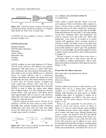
Figure 13.8 LOCOS (a) before oxidation: thin pad oxide stresses, and this causes a number of pattern-dependent
and patterned nitride and (b) after oxidation: no oxidation phenomena that can be either beneficial or disadvanta-
under nitride but ‘bird’s beak’ at nitride edge geous. Typical stress values are of the order of 300 MPa.
◦
Somewhere between 975 and 1000 C, the oxide exhibits
viscous flow. Oxidation above that temperature will
as LOCOS, for local oxidation of silicon. LOCOS is
result in reduced stress and wafer bow. Below that
pictured in Figure 13.8.
temperature, oxide needs to be treated as an elastic
material with appropriate elastic constants. Scaling of
LOCOS process flow LOCOS to smaller linewidths meets an inevitable limit
at sub-micron dimensions: stresses in the growing oxide
thermal oxidation; prevent full oxidation of narrow gaps. For generations
LPCVD nitride deposition; below 0.5 µm linewidths, the isolation method of choice
lithography;
is shallow trench isolation (STI), which will be discussed
nitride etching;
in Chapter 25.
photoresist strip;
Thermal oxidation of small silicon wires shows a
cleaning;
self-limiting effect due to high stresses and this has
oxidation.
been utilized in making nanostructures. This is illus-
trated in the silicon-on-insulator (SOI) nanowire process
LOCOS variables are pad oxide thickness (10–50 nm), (Figure 13.10).
LPCVD nitride thickness (100–200 nm) and oxidation
temperature. Pad oxide serves as a stress relief layer,
and it diminishes the stress-induced dislocations that a Process flow for silicon nanowires
thick nitride exerts in silicon. Nitride acts as a diffusion SOI wafer with 21 nm thick device silicon;
barrier for oxygen diffusion, and as a mechanical lithography;
stiffener: the thicker the nitride, the smaller the oxide silicon etching;
growth under the mask. This lateral extension is known photoresist striping;
as bird’s beak, for obvious reasons. A thinner pad oxidation.
oxide would help minimize bird’s beak but at the
expense of silicon damage from nitride stress. Recessed Thermal oxidation proceeds for a while, but then a self-
LOCOS is used to make the surface more planar limiting effect sets in: a critical stress, which stops
after oxidation (Figure 13.9). The etching step involves oxidation, is ca. 2.6 GPa at 850 C. After the self-
◦
etching nitride, oxide and silicon, with silicon etched limiting oxide thickness has been grown, no further
depth approximately half the desired oxide thickness, oxidation takes place. If oxidation is carried out at
which then will result in approximately equal surface a higher temperature, say 1000 C, this stress can be
◦
heights for oxide and silicon. overcome, and the whole structure will be oxidized
LOCOS isolation has been used for 30 years for its (Figure 13.10).
simplicity. LOCOS has been scaled to much smaller Stresses are also responsible for non-uniform oxi-
linewidths than anybody thought possible. Numerous dation in convex and concave corners as shown in
modifications have been tried, but most have failed Figure 13.11. Uneven oxide thickness causes problems
because the added process complexity has not offered for reliability because electric field strength is differ-
enough improvement in isolation. ent in corners and planar areas. Etched trenches have
concave corners, and therefore both STI and DRAM
trench capacitors require fine-tuning of the bottom cor-
ners if thermal oxidation is used as the first film in the
trench. Etch processes can be tailored to some extent
(a) (b) (c) for smoother bottom profiles, but this is a limited option
Figure 13.9 Bird’s beak in LOCOS (a) thin nitride; (b) because the top corner needs rounding too. Oxide and
thick nitride and (c) recessed LOCOS nitride can be deposited by conformal CVD, but in very