
Page 170 - Sami Franssila Introduction to Microfabrication
P. 170
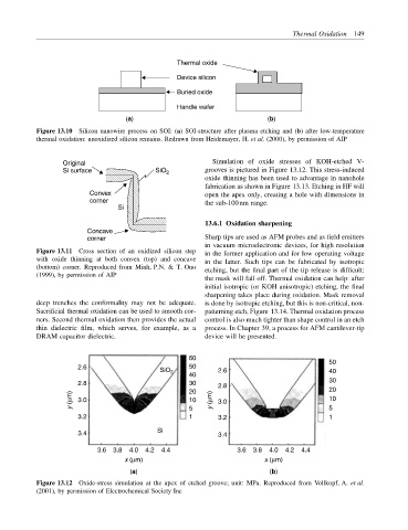
Thermal Oxidation 149


                                               Thermal oxide
                                               Device silicon
                                               Buried oxide

                                               Handle wafer
                                  (a)                                  (b)
           Figure 13.10 Silicon nanowire process on SOI: (a) SOI-structure after plasma etching and (b) after low-temperature
           thermal oxidation: unoxidized silicon remains. Redrawn from Heidemayer, H. et al. (2000), by permission of AIP


                  Original                               Simulation of oxide stresses of KOH-etched V-
                  Si surface              SiO 2        grooves is pictured in Figure 13.12. This stress-induced
                                                       oxide thinning has been used to advantage in nanohole
                                                       fabrication as shown in Figure 13.13. Etching in HF will
                         Convex                        open the apex only, creating a hole with dimensions in
                         corner                        the sub-100 nm range.
                                Si

                                                       13.6.1 Oxidation sharpening
                        Concave
                        corner                         Sharp tips are used as AFM probes and as field emitters
                                                       in vacuum microelectronic devices, for high resolution
           Figure 13.11 Cross section of an oxidized silicon step  in the former application and for low operating voltage
           with oxide thinning at both convex (top) and concave  in the latter. Such tips can be fabricated by isotropic
           (bottom) corner. Reproduced from Minh, P.N. & T. Ono
                                                       etching, but the final part of the tip release is difficult:
           (1999), by permission of AIP
                                                       the mask will fall off. Thermal oxidation can help: after
                                                       initial isotropic (or KOH anisotropic) etching, the final
                                                       sharpening takes place during oxidation. Mask removal
           deep trenches the conformality may not be adequate.  is done by isotropic etching, but this is non-critical, non-
           Sacrificial thermal oxidation can be used to smooth cor-  patterning etch, Figure 13.14. Thermal oxidation process
           ners. Second thermal oxidation then provides the actual  control is also much tighter than shape control in an etch
           thin dielectric film, which serves, for example, as a  process. In Chapter 39, a process for AFM cantilever-tip
           DRAM capacitor dielectric.                  device will be presented.

                                                   60
                     2.6                   SiO 2   50     2.6                          50
                                                                                       40
                                                   40
                     2.8                           30     2.8                          30
                                                   20                                  20
                    y (µm)  3.0                    10    y (µm)  3.0                   10
                                                                                       5
                                                   5
                     3.2                           1      3.2                          1
                     3.4                  Si              3.4

                           3.6  3.8  4.0  4.2  4.4             3.6  3.8  4.0  4.2  4.4
                                  x (µm)                              x (µm)
                                   (a)                                  (b)
           Figure 13.12 Oxide-stress simulation at the apex of etched groove; unit: MPa. Reproduced from Vollkopf, A. et al.
           (2001), by permission of Electrochemical Society Inc