Page 206 - Sami Franssila Introduction to Microfabrication
P. 206

Moulding and Stamping 185


                                                           Oxide

                                                                Polysilicon
                                                                               (a)


                                                                                Cu
                                                                               (b)


                                                           Anchor


                                                             Tether
                                                                               (c)


                                                                        Solder bump

                                                                          Target die
                                                                               (d)


                                                                               (e)


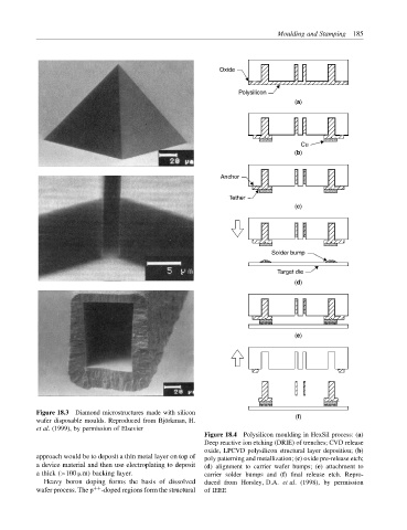
           Figure 18.3 Diamond microstructures made with silicon               (f)
           wafer disposable moulds. Reproduced from Bj¨ orkman, H.
           et al. (1999), by permission of Elsevier
                                                       Figure 18.4 Polysilicon moulding in HexSil process: (a)
                                                       Deep reactive ion etching (DRIE) of trenches; CVD release
                                                       oxide, LPCVD polysilicon structural layer deposition; (b)
           approach would be to deposit a thin metal layer on top of  poly patterning and metallization; (c) oxide pre-release etch;
           a device material and then use electroplating to deposit  (d) alignment to carrier wafer bumps; (e) attachment to
           a thick (>100 µm) backing layer.            carrier solder bumps and (f) final release etch. Repro-
             Heavy boron doping forms the basis of dissolved  duced from Horsley, D.A. et al. (1998), by permission
           wafer process. The p ++ -doped regions form the structural  of IEEE
   201   202   203   204   205   206   207   208   209   210   211