
Page 205 - Sami Franssila Introduction to Microfabrication
P. 205
184 Introduction to Microfabrication
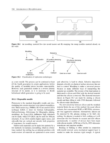
(a) (b)
Figure 18.1 (a) moulding: material flow into mould master and (b) stamping: the stamp modifies material already on
the wafer
Moulding
Stamping
Re-usable Disposable 2D surface stamping 3D volume stamping
(soft stamp)
(rigid stamp)
Surface Inking Catalyst Used as a mask Used as such
modification
Figure 18.2 Classification of replication technologies
as a new mould. This process can be continued at least and selectivity is hard to obtain. Selective deposition
till the fourth generation in certain applications, before depends critically on chemical surface processes that are
the quality of moulded pieces becomes unacceptable. hard to control. Moulding is rather a universal process
However, each generation results in a reverse polarity because so many different ways of transporting the
structure of its parent, so it is necessary to decide material are available. The reverse of the final pattern is
beforehand which generation is going to be used. fabricated in silicon and filled with the desired material
and then the silicon is removed. The diamond structures
shown in Figure 18.3 are made by etching a silicon
18.1.1 Disposable moulds
mould and then filling it with CVD diamond, followed
Photoresist is the standard disposable mould, and elec- by silicon wafer dissolution.
troplating into a resist structure is its typical exemplifica- The etch selectivity between silicon and the moulded
tion. Thick resists (e.g., PMMA, SU-8) are used in LIGA material limits the use of this method: the usual silicon
technique (LIGA is short for German Lithographie, etchants, hot concentrated KOH or HF:HNO 3 mixtures,
Galvanoformung, Abformung; for lithography, plating, are very aggressive solutions. Alternatively, silicon can
moulding). In X-ray-LIGA millimetre high structures be removed by SF 6 plasma etching or by XeF 2 dry
can be made, while UV-LIGA can be used for 500 µm etching. No plasma is needed in XeF 2 etching as it will
structures. X-ray LIGA enables higher aspect ratios, and dissociate into free fluorine in vacuum and etch silicon
sidewalls that are vertical and smooth, both properties spontaneously. A number of devices have been made
of importance for mould masters. with silicon moulds: AFM tips of Si 3 N 4 , PZT-ultrasonic
Hard-to-etch materials can be made into patterns by a transducers and parylene needles.
few methods: for instance, ion milling, which is a brute- Backing or bulking is often needed in connection
force method. Ion milling has an inherent problem with with mould removal: some mechanical support layer is
mask erosion: all materials are sputtered to some extent needed to make the structure rigid enough. A typical