
Page 215 - Sami Franssila Introduction to Microfabrication
P. 215
194 Introduction to Microfabrication
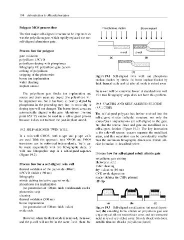
Polygate MOS process flow Phosphorous implant Boron implant
The first major self-aligned structure to be implemented
was the polysilicon gate, which rapidly replaced the non-
self-aligned aluminium gate.
Process flow for polygate n-well p-well
gate oxidation (a) (b)
polysilicon LPCVD
polysilicon doping with phosphorus
lithography #1: polysilicon gate pattern
etching of polysilicon (c)
stripping of the photoresist Figure 19.2 Self-aligned twin well: (a) phosphorus
boron ion implantation implant blocked by nitride; (b) boron implant blocked by
wafer cleaning thick thermal oxide and (c) after all oxide is etched away
implant anneal.
the n-well will be somewhat lower. A standard twin well
The polysilicon gate blocks ion implantation and
with two lithography steps does not have this problem.
source and drain areas are doped (the polysilicon will
be implanted too, but it has been so heavily doped by
phosphorus in the preceding step that its resistivity or 19.3 SPACERS AND SELF-ALIGNED SILICIDE
doping type will not change). The boron-doped areas are (SALICIDE)
automatically aligned to the gate. Aluminium (melting The self-aligned polygate has further evolved into the
◦
point 653 C) cannot be used in a self-aligned process self-aligned-silicide (salicide) structure: not only the
because it does not tolerate the post-implant anneal.
source/drain implantations are self-aligned to the gate,
but also the source, drain and gate are metallized in a
19.2 SELF-ALIGNED TWIN WELL self-aligned fashion (Figure 19.3). The key innovation
is the sidewall spacer: spacers separate the metallized
In a twin-well CMOS, both n-type and p-type wells areas, and this separation can be considerably smaller
are used. With this approach, both NMOS and PMOS than the minimum lithographic dimension. Cobalt sili-
transistors can be optimized independently. Wells can cide formation is described below.
be made sequentially with two lithographic steps, or
with one lithographic step in a self-aligned sequence
(Figure 19.2). Process flow for self-aligned cobalt silicide gate
polysilicon gate etching
photoresist strip
Process flow for a self-aligned twin well
wafer cleaning
thermal oxidation of the pad oxide (40 nm) dry oxidation (10 nm)
LPCVD nitride (150 nm) CVD oxide deposition
lithography spacer etching (in CHF 3 plasma)
nitride etching (selective against oxide) HF-dip
phosphorus ion implantation
(no penetration of 190 nm thick nitride/oxide stack)
photoresist strip
cleaning
thermal oxidation (500 nm)
boron implantation (a) (b) (c)
(no penetration of 500 nm thick oxide) Figure 19.3 Self-aligned metallization: (a) metal deposi-
oxide etch. tion; (b) annealing forms silicide on polysilicon gate and
single-crystal silicon source/drain areas and (c) unreacted
However, when the thick oxide is removed, the n-well metal is selectively etched away. Silicide (black with dots),
and the p-well will not be in the same focus plane, but metallic titanium (black), polysilicon (dotted)