
Page 245 - Sami Franssila Introduction to Microfabrication
P. 245
224 Introduction to Microfabrication
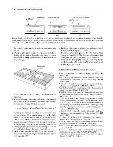
n-diffusion Porous silicon Single crystal silicon
p-diffusion Cavity
p-silicon 10 ohm-cm p-silicon 10 ohm-cm p-silicon 10 ohm-cm
(a) (b) (c)
Figure 22.15 (a) A shallow n-diffusion and a deeper p-diffusion; (b) lateral porous silicon formation in the heavily
boron-doped region and (c) dilute KOH sacrificial etching releases a single-crystalline n-silicon bridge. Redrawn after
Lee, C.-S., Lee, J.-D. & Han, C.-H. (2000), by permission of Elsevier
be smaller than nitride deposition non-uniformity 6. Design a fabrication process for the polymer hinged
of 3%? mirror shown in Figure 22.12(a).
2. Design a fabrication process for the suspended silicon 7. Design a fabrication process for the fluidic filter
bridge shown below. Consider two cases: a bridge shown in Figure 22.1. Also draw the photomasks that
made of LPCVD polysilicon and a SOI device silicon show how the filter is anchored to the substrate.
layer bridge. 8. What are the lithography steps and sacrificial layers
needed to make a 3D coil with a Ni core (transformer)
shown in Figure 22.9(b)?
Suspended
part
REFERENCES AND RELATED READINGS
Bellet, D. & Canham, L.: Controlled drying, Adv. Mater., 10
(1998), 487.
Si
Bruschi, P. et al: Micromachined silicon suspended wires with
submicrometric dimensions, Microelectron. Eng., 57–58
SiO 2
(2001), 959.
Si Bustillo, J. et al: Surface micromachining for microelectrome-
chanical systems, IEEE Proc., 86 (1998), 1559.
Chu, W.-H. et al: Silicon membrane nanofilters from sacrificial
oxide removal, J. MEMS, 8 (1999), 34.
Hedrich, F., Billat, S. & Lang, W.: Structuring of membrane
From Bruschi, P. et al. (2001), by permission of sensors using sacrificial porous silicon, Sensors Actuators,
Elsevier. 84 (2000), 315.
Lammel, G. & Renaud, Ph.: Free-standing mobile 3D porous
3. Comb-drive fabrication tolerance: resonant frequency
silicon microstructures, Sensors Actuators, 85 (2000), 356.
of a surface micromachined resonator with straight
Lee, C.-S., Lee, J.-D. & Han, C.-H.: A new wide-dimensional
flexures (see Figure 22.4(a)) is given by
freestanding microstructure fabrication technology using
laterally formed porous silicon as a sacrificial layer, Sensors
3
3
f 0 = (1/2π){(4EtW /ML ) + (24σ r Wt/5ML)} 1/2 Actuators, 84 (2000), 181.
L¨ ochel, B. et al: Ultraviolet depth lithography and gal-
where E is Young’s modulus, σ r is residual stress vanoforming for micromachining, J. Electrochem. Soc., 143
in polysilicon, M is shuttle mass, t is poly thick- (1996), 237.
ness, L is flexure length and W is flexure width. Mehregany, M. & Dewa, A.S.: http://mems.cwru.edu/short-
What is the effect of fabrication tolerance on reso- course/, Case Western Reserve University.
nance frequency? Consider poly thickness and lithog- Orvis, W.J. et al: Modeling and fabricating microcavity inte-
grated vacuum tubes, IEEE TED, 36 (1989), 2651.
raphy/etching variation for some realistic dimensions.
Pister, K. et al: Microfabricated hinges, Sensors Actuators,
4. Design proper thicknesses and etched depths to make A33 (1992), 249.
the self-aligned rotor shown in Figure 22.11. Roy, S. et al: Fabrication and characterization of polycrys-
5. How many photolithography steps are needed to talline SiC resonators, IEEE TED, 49 (2002), 2323.
make the polysilicon-hinged mirror structure shown Suzuki, K. et al: Insect-model based microrobot with elastic
in Figure 22.13? hinges, J. MEMS, 3 (1994), 5.