
Page 249 - Sami Franssila Introduction to Microfabrication
P. 249
228 Introduction to Microfabrication
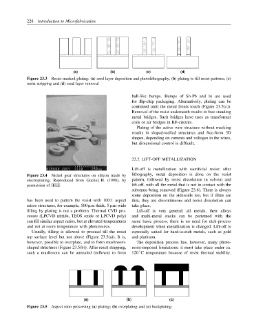
(a) (b) (c) (d)
Figure 23.3 Resist masked plating: (a) seed layer deposition and photolithography; (b) plating to fill resist patterns; (c)
resist stripping and (d) seed layer removal
ball-like bumps. Bumps of Sn-Pb and In are used
for flip-chip packaging. Alternatively, plating can be
continued until the metal fronts touch (Figure 23.5(c)).
Removal of the resist underneath results in free-standing
metal bridges. Such bridges have uses as transformer
coils or air bridges in RF-circuits.
Plating of the active wire structure without masking
results in sloped-walled structures and free-form 3D
shapes, depending on currents and voltages in the wires,
but dimensional control is difficult.
23.2 LIFT-OFF METALLIZATION
Lift-off is metallization with sacrificial resist: after
Figure 23.4 Nickel gear structures on silicon made by lithography, metal deposition is done on the resist
electroplating. Reproduced from Guckel, H. (1998), by pattern, followed by resist dissolution in solvent and
permission of IEEE lift-off, with all the metal that is not in contact with the
substrate being removed (Figure 23.6). There is always
some deposition on the sidewalls too, but if films are
has been used to pattern the resist with 100:1 aspect thin, they are discontinuous and resist dissolution can
ratios structures, for example, 500 µm thick, 5 µm wide take place.
filling by plating is not a problem. Thermal CVD pro- Lift-off is very general: all metals, their alloys
cesses (LPCVD nitride, TEOS oxide or LPCVD poly) and multi-metal stacks can be patterned with the
can fill similar aspect ratios, but at elevated temperatures same basic process; there is no need for etch-process
and not at room temperature with photoresists. development when metallization is changed. Lift-off is
Usually, filling is allowed to proceed till the resist especially suited for hard-to-etch metals, such as gold
top surface level but not above (Figure 23.5(a)). It is, and platinum.
however, possible to overplate, and to form mushroom- The deposition process has, however, many photo-
shaped structures (Figure 23.5(b)). After resist stripping, resist-imposed limitations: it must take place under ca.
◦
such a mushroom can be annealed (reflown) to form 120 C temperature because of resist thermal stability.
(a) (b) (c)
Figure 23.5 Aspect ratio preserving (a) plating; (b) overplating and (c) backplating