
Page 254 - Sami Franssila Introduction to Microfabrication
P. 254
Structures by Deposition 233
Anode (poly–Si)
Vacuum micro–cavity
Gate Gate Mo/Oxide
(Mo) (Mo) Cathode
Poly–Si
Anode Upper insulator
Lower insulator
Cathode (poly–Si)
(a) (b)
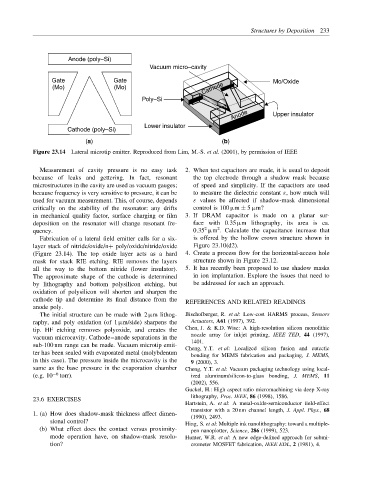
Figure 23.14 Lateral microtip emitter. Reproduced from Lim, M.-S. et al. (2001), by permission of IEEE
Measurement of cavity pressure is no easy task 2. When test capacitors are made, it is usual to deposit
because of leaks and gettering. In fact, resonant the top electrode through a shadow mask because
microstructures in the cavity are used as vacuum gauges; of speed and simplicity. If the capacitors are used
because frequency is very sensitive to pressure, it can be to measure the dielectric constant ε, how much will
used for vacuum measurement. This, of course, depends ε values be affected if shadow-mask dimensional
critically on the stability of the resonator: any drifts control is 100 µm ± 5 µm?
in mechanical quality factor, surface charging or film 3. If DRAM capacitor is made on a planar sur-
deposition on the resonator will change resonant fre- face with 0.35 µm lithography, its area is ca.
2
2
quency. 0.35 µm . Calculate the capacitance increase that
Fabrication of a lateral field emitter calls for a six- is offered by the hollow crown structure shown in
layer stack of nitride/oxide/n+ poly/oxide/nitride/oxide Figure 23.10(d2).
(Figure 23.14). The top oxide layer acts as a hard 4. Create a process flow for the horizontal-access hole
mask for stack RIE etching. RIE removes the layers structure shown in Figure 23.12.
all the way to the bottom nitride (lower insulator). 5. It has recently been proposed to use shadow masks
The approximate shape of the cathode is determined in ion implantation. Explore the issues that need to
by lithography and bottom polysilicon etching, but be addressed for such an approach.
oxidation of polysilicon will shorten and sharpen the
cathode tip and determine its final distance from the
REFERENCES AND RELATED READINGS
anode poly.
The initial structure can be made with 2 µm lithog- Bischofberger, R. et al: Low-cost HARMS process, Sensors
raphy, and poly oxidation (of 1 µm/side) sharpens the Actuators, A61 (1997), 392.
tip. HF etching removes polyoxide, and creates the Chen, J. & K.D. Wise: A high-resolution silicon monolithic
nozzle array for inkjet printing, IEEE TED, 44 (1997),
vacuum microcavity. Cathode–anode separations in the
1401.
sub-100 nm range can be made. Vacuum microtip emit-
Cheng, Y.T. et al: Localized silicon fusion and eutectic
ter has been sealed with evaporated metal (molybdenum bonding for MEMS fabrication and packaging, J. MEMS,
in this case). The pressure inside the microcavity is the 9 (2000), 3.
same as the base pressure in the evaporation chamber Cheng, Y.T. et al: Vacuum packaging technology using local-
(e.g. 10 −6 torr). ized aluminum/silicon-to-glass bonding, J. MEMS, 11
(2002), 556.
Guckel, H.: High aspect ratio micromachining via deep X-ray
23.6 EXERCISES lithography, Proc. IEEE, 86 (1998), 1586.
Hartstein, A. et al: A metal-oxide-semiconductor field-effect
transistor with a 20 nm channel length, J. Appl. Phys., 68
1. (a) How does shadow-mask thickness affect dimen- (1990), 2493.
sional control? Hing, S. et al: Multiple ink nanolithography: toward a multiple-
(b) What effect does the contact versus proximity- pen nanoplotter, Science, 286 (1999), 523.
mode operation have, on shadow-mask resolu- Hunter, W.R. et al: A new edge-defined approach for submi-
tion? crometer MOSFET fabrication, IEEE EDL, 2 (1981), 4.