
Page 259 - Sami Franssila Introduction to Microfabrication
P. 259
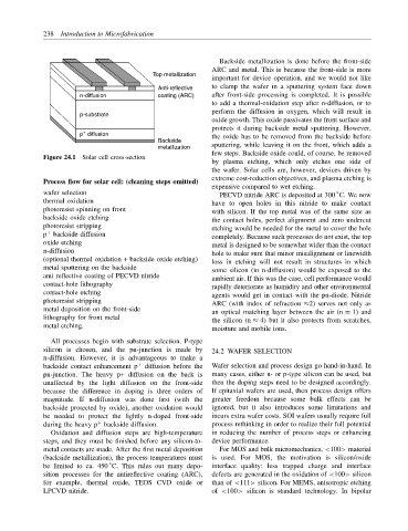
238 Introduction to Microfabrication


                                                           Backside metallization is done before the front-side
                                                         ARC and metal. This is because the front-side is more
                                         Top metallization
                                                         important for device operation, and we would not like
                                           Anti-reflective  to clamp the wafer in a sputtering system face down
                      n-diffusion          coating (ARC)  after front-side processing is completed. It is possible
                                                         to add a thermal-oxidation step after n-diffusion, or to
                                                         perform the diffusion in oxygen, which will result in
                      p-substrate
                                                         oxide growth. This oxide passivates the front surface and
                                                         protects it during backside metal sputtering. However,
                       +
                      p  diffusion                       the oxide has to be removed from the backside before
                                           Backside
                                           metallization  sputtering, while leaving it on the front, which adds a
                                                         few steps. Backside oxide could, of course, be removed
            Figure 24.1 Solar cell cross-section
                                                         by plasma etching, which only etches one side of
                                                         the wafer. Solar cells are, however, devices driven by
                                                         extreme cost-reduction objectives, and plasma etching is
            Process flow for solar cell: (cleaning steps omitted)
                                                         expensive compared to wet etching.
            wafer selection                                PECVD nitride ARC is deposited at 300 C. We now
                                                                                         ◦
            thermal oxidation                            have to open holes in this nitride to make contact
            photoresist spinning on front                with silicon. If the top metal was of the same size as
            backside oxide etching                       the contact holes, perfect alignment and zero undercut
            photoresist stripping                        etching would be needed for the metal to cover the hole
             +
            p backside diffusion                         completely. Because such processes do not exist, the top
            oxide etching                                metal is designed to be somewhat wider than the contact
            n-diffusion                                  hole to make sure that minor misalignment or linewidth
            (optional thermal oxidation + backside oxide etching)  loss in etching will not result in structures in which
            metal sputtering on the backside             some silicon (in n-diffusion) would be exposed to the
            anti reflective coating of PECVD nitride      ambient air. If this was the case, cell performance would
            contact-hole lithography
                                                         rapidly deteriorate as humidity and other environmental
            contact-hole etching
                                                         agents would get in contact with the pn-diode. Nitride
            photoresist stripping                        ARC (with index of refraction ≈2) serves not only as
            metal deposition on the front-side           an optical matching layer between the air (n = 1) and
            lithography for front metal                  the silicon (n ≈ 4) but it also protects from scratches,
            metal etching.
                                                         moisture and mobile ions.
              All processes begin with substrate selection. P-type
            silicon is chosen, and the pn-junction is made by  24.2 WAFER SELECTION
            n-diffusion. However, it is advantageous to make a
            backside contact enhancement p +  diffusion before the  Wafer selection and process design go hand-in-hand. In
            pn-junction. The heavy p+ diffusion on the back is  many cases, either n- or p-type silicon can be used, but
            unaffected by the light diffusion on the front-side  then the doping steps need to be designed accordingly.
            because the difference in doping is three orders of  If epitaxial wafers are used, then process design offers
            magnitude. If n-diffusion was done first (with the  greater freedom because some bulk effects can be
            backside protected by oxide), another oxidation would  ignored, but it also introduces some limitations and
            be needed to protect the lightly n-doped front-side  incurs extra wafer costs. SOI wafers usually require full
                           +
            during the heavy p backside diffusion.       process rethinking in order to realize their full potential
              Oxidation and diffusion steps are high-temperature  in reducing the number of process steps or enhancing
            steps, and they must be finished before any silicon-to-  device performance.
            metal contacts are made. After the first metal deposition  For MOS and bulk micromechanics, <100> material
            (backside metallization), the process temperatures must  is used. For MOS, the motivation is silicon/oxide
            be limited to ca. 450 C. This rules out many depo-  interface quality: less trapped charge and interface
                              ◦
            sition processes for the antireflective coating (ARC),  defects are generated in the oxidation of <100> silicon
            for example, thermal oxide, TEOS CVD oxide or  than of <111> silicon. For MEMS, anisotropic etching
            LPCVD nitride.                               of <100> silicon is standard technology. In bipolar