
Page 264 - Sami Franssila Introduction to Microfabrication
P. 264
Process Integration 243
layer-to-layer positioning. These are often referred to space: it is typical that, for example, a 0.5 µm linewidth
as layout rules, as opposed to electrical design rules process has a 0.5 µm minimum line and a 0.7 µm mini-
that include information about sheet resistances, current mum space. Sometimes processes are specified by half-
density limitations, contact resistances and so on. Layer- pitch: the previous process would then be classified as
thickness design rules are needed in a capacitor design: a 0.6 µm process.
oxide thickness determines capacitance density, both The final structure width is determined by process
when the oxide is used as a capacitor dielectric as step properties. Diffusion is an isotropic process and a
such, and when it is used as a sacrificial layer in the 3 µm diffusion depth leads to ca. 3 µm lateral spreading.
fabrication of an air-gap capacitor. Device models (for Similarly, isotropic etch undercutting necessitates simi-
transistors, resistors, capacitors) are additional higher- lar design concerns: equal spacing of 10 µm wide, 5 µm
level abstractions of the process for circuit designers. deep grooves would result in touching of the neighbour-
Design rules and models are always process specific. ing grooves.
They are also company specific: 0.13 µm CMOS Device interactions come in many guises and they
processes from different suppliers have different sets of are device and process specific. Transistors need to
rules and models. be isolated from each other, and this isolation takes
up space. Inductive devices must be placed far away
from each other because of magnetic field coupling over
24.4.1 Layout rules distance. It is also important to understand and to limit
structures that can be placed between two coils as these
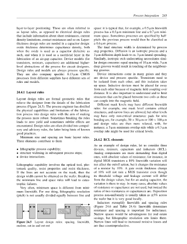
Layout design rules are formal geometric rules that can couple into the magnetic field.
relieve the designer from the details of the fabrication Different mask levels may have different linewidth
process (Figure 24.5). The process engineer has distilled rules: for example, one mask level contains critical
the physical capabilities and limitations of the fabrica- structures, and narrow lines are allowed, but other levels
tion process into design rules with the aim of making may have only non-critical structures: pads for wire
the process more robust. Sometimes breaking the rules bonding are, for example, 50 × 50 µm or 100 × 100 µm
leads to zero yield and sometimes subtler effects are and design rules are then more relaxed, with, for
encountered. Design rules are often divided into compul- instance, a 5 µm minimum overlap rule while a 0.3 µm
sory and advisory rules, the latter being hints of known overlap rule might be used for critical levels.
good practices.
Minimum size and spacing are basic layout rules.
Three elements contribute to them 24.4.2 RCL elements
As an example of design rules, let us consider three
• lithographic process capability; devices, resistors, capacitors and inductors (RCL).
• structure widening in subsequent process steps; Analog components are more demanding than digital
• device interactions. ones, with absolute values of resistance; for instance, in
digital MOS transistors a 10% linewidth variation will
Lithographic capability involves the optical tool, pho- not affect the on/off action, but it changes the resistance
tomask quality, resist properties and resist thickness. of a resistor by 10%. A gate oxide thickness change
If the lines are not accurate on the mask, then the of 10% will not ruin a MOS transistor even though
design width cannot be obtained on the wafer. Breaking its threshold voltage and leakage current will differ
the minimum line and space rules will lead to catas- from the design values, but for an analog capacitor, the
trophic failures. variation is there to stay. In many cases, absolute values
Very often, minimum space is different from mini- of resistance or capacitance are not used, but instead the
mum linewidth. For one thing, lithographic resolution ratios of two resistances or capacitances are. Deposition
(pitch) is not usually divided equally between line and process non-uniformity is usually taken as ±5% across
the wafer but it is very good locally.
Inductors exemplify linewidth and spacing rules
(Figure 24.6 and Table 24.4): linewidth determines
resistance and spacing is important for inductance.
Narrow spaces would be advantageous for real estate
savings, but lithographic resolution sets limits there.
Figure 24.5 Layout design rules: spacing, linewidth, Narrow lines will lead to increased resistive losses and
enclose, cut-in and cut-out are thus counterproductive.