
Page 261 - Sami Franssila Introduction to Microfabrication
P. 261
240 Introduction to Microfabrication
develop during high temperature process steps or result Devices
from ingot sawing and lapping operations. The presence (≈ 5 µm)
of excessive thickness variation and warp, will affect the Denuded zone
lithographic performance via depth-of-focus problems. (≈ 20 µm)
Wafer surface topography can be divided into a few
Wafer bulk
distinct scales: roughness is in the micron scale, flatness
(oxygen
is in the chip scale and bow and warp are in the wafer precipitates)
scale. Smoothness and flatness are essential parameters
for fusion bonding: wafers with 0.1 nm roughness are
Backside getter
preferred for fusion bonding. Anodic bonding is more (≈ 1 µm)
forgiving to surface roughness, and wafers with 0.5 nm
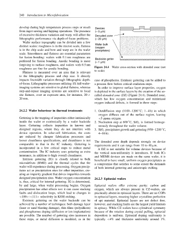
Figure 24.4 Wafer cross-section with denuded zone (not
roughness are fine for anodic bonding.
to scale)
Flatness is measured over an area that is relevant
to the lithography process and chip size. It directly
impacts linewidth variation through lithographic depth- case of phosphorus. Extrinsic gettering can be added to
of-focus. Lithographic processes utilizing 1X full wafer- a process flow before critical oxidation steps.
imaging systems are sensitive to global flatness, whereas In order to improve surface layer properties, oxygen
step-and-repeat imaging systems are sensitive to local is depleted in the surface layers by the creation of the so-
site flatness, over an exposure area, for instance, 20 × called denuded zone (DZ) (Figure 24.4). Denuded zone,
20 mm. which has low oxygen concentration and minimized
oxygen induced defects, is formed in three steps:
◦
24.2.2 Wafer behaviour in thermal treatments 1. Outdiffusion step (1100–1200 C; 1–4 h) in which
oxygen diffuses out of the surface region, leaving
Gettering is the trapping of impurities either intrinsically <5 ppma oxygen.
inside the wafer or extrinsically by a wafer backside 2. Nucleation step at 600 C, SiO x is formed homoge-
◦
layer. Gettering collects impurities in known and neously throughout the wafer volume.
designed regions, where they do not interfere with 3. SiO x precipitates growth and gettering (950–1200 C,
◦
device operation. In solar-cell fabrication, the costs 4–16 h).
are reduced by cheaper fabrication processes and
looser cleanliness specifications, and cleanliness is not
The denuded zone depth depends strongly on device
comparable to that in the IC industry. Gettering is
requirements and it can range from 10 to 40 µm.
incorporated in a few critical steps to reduce metal
A DZ is not suitable for volume devices because of
contamination. The IC industry uses gettering as extra
the vertical non-uniformity it introduces. If both ICs
insurance, in addition to high overall cleanliness.
and MEMS devices are made on the same wafer, it is
Intrinsic gettering (IG) is closely related to bulk
beneficial to have small, uniform oxygen precipitates as
microdefects (BMD) and the thermal cycles that the
a compromise that satisfies to some extent the demands
wafer will experience during processing. Oxygen precip-
of both internal gettering and anisotropic etching.
itates act as precipitation sites for other impurities, cre-
ating an impurity gradient that drives impurities towards
designed precipitation sites. Wafer oxygen concentration 24.2.3 Epitaxial wafers
is, thus, critical for internal gettering. IG is determined,
by and large, when wafer processing begins. Oxygen Epitaxial wafers offer extreme purity: carbon and
precipitation has other effects too: it can cause stacking oxygen, which are always present in CZ-wafers, are
faults and dislocation loops, which lead to changes in practically absent in epitaxial layers. There are no COPs
<100>:<111> selectivity in KOH etching. in epitaxial layers, meaning higher crystalline perfection
Extrinsic gettering on the wafer backside can be of epi material. Epitaxial layers are not defect free,
achieved by a number of techniques: both damage layer however, and stacking faults are the largest yield limiters
(laser or sand blasting damage), thin films (polysilicon) in epitaxy. While CZ-wafers have cylindrical symmetry
and phosphorous doping (diffusion or ion implantation) because of the rotation during crystal pulling, epitaxial
are possible. The number of gettering sites increases in deposition is uniform. Epitaxial doping uniformity is
these steps, or metal diffusion is modified, as in the typically <4% and thickness uniformity around 1%.