
Page 265 - Sami Franssila Introduction to Microfabrication
P. 265
244 Introduction to Microfabrication
Table 24.5 Design rules for a polysilicon thin-film
resistor
Resistor lines 3 µm
Space 3 µm
A A′ High-resistivity poly 5000 ohm/sq
Low-resistivity poly 500 ohm/sq
◦
Only 90 corners allowed in
meandering resistors
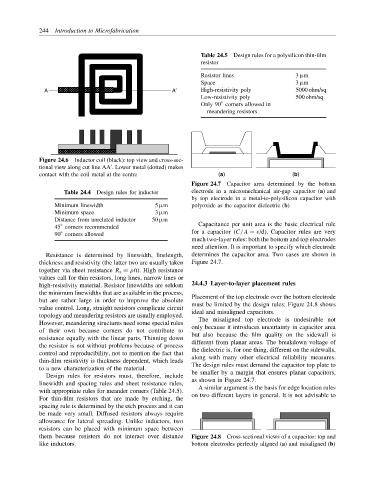
Figure 24.6 Inductor coil (black): top view and cross-sec-
′
tional view along cut line AA . Lower metal (dotted) makes
contact with the coil metal at the centre (a) (b)
Figure 24.7 Capacitor area determined by the bottom
Table 24.4 Design rules for inductor electrode in a micromechanical air-gap capacitor (a) and
by top electrode in a metal-to-polysilicon capacitor with
Minimum linewidth 5 µm polyoxide as the capacitor dielectric (b)
Minimum space 3 µm
Distance from unrelated inductor 50 µm
◦
45 corners recommended Capacitance per unit area is the basic electrical rule
◦
90 corners allowed for a capacitor (C/A = ε/d). Capacitor rules are very
much two-layer rules: both the bottom and top electrodes
need attention. It is important to specify which electrode
Resistance is determined by linewidth, linelength, determines the capacitor area. Two cases are shown in
thickness and resistivity (the latter two are usually taken Figure 24.7.
together via sheet resistance R s ≡ ρ/t). High resistance
values call for thin resistors, long lines, narrow lines or
high-resistivity material. Resistor linewidths are seldom 24.4.3 Layer-to-layer placement rules
the minimum linewidths that are available in the process, Placement of the top electrode over the bottom electrode
but are rather large in order to improve the absolute must be limited by the design rules: Figure 24.8 shows
value control. Long, straight resistors complicate circuit ideal and misaligned capacitors.
topology and meandering resistors are usually employed. The misaligned top electrode is undesirable not
However, meandering structures need some special rules only because it introduces uncertainty in capacitor area
of their own because corners do not contribute to
but also because the film quality on the sidewall is
resistance equally with the linear parts. Thinning down
different from planar areas. The breakdown voltage of
the resistor is not without problems because of process
the dielectric is, for one thing, different on the sidewalls,
control and reproducibility, not to mention the fact that
along with many other electrical reliability measures.
thin-film resistivity is thickness dependent, which leads
The design rules must demand the capacitor top plate to
to a new characterization of the material.
Design rules for resistors must, therefore, include be smaller by a margin that ensures planar capacitors,
linewidth and spacing rules and sheet resistance rules, as shown in Figure 24.7.
with appropriate rules for meander corners (Table 24.5). A similar argument is the basis for edge location rules
For thin-film resistors that are made by etching, the on two different layers in general. It is not advisable to
spacing rule is determined by the etch process and it can
be made very small. Diffused resistors always require
allowance for lateral spreading. Unlike inductors, two
resistors can be placed with minimum space between
them because resistors do not interact over distance Figure 24.8 Cross-sectional views of a capacitor: top and
like inductors. bottom electrodes perfectly aligned (a) and misaligned (b)