
Page 268 - Sami Franssila Introduction to Microfabrication
P. 268
Process Integration 247
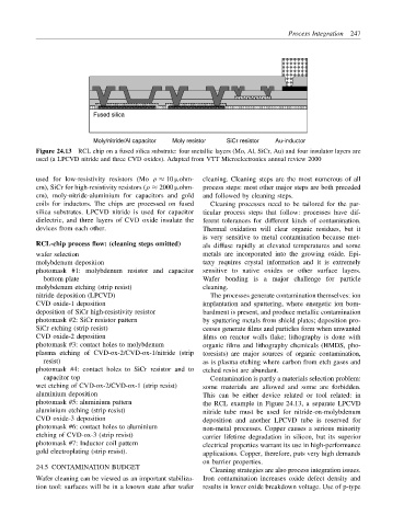
Fused silica
Moly/nitride/Al capacitor Moly resistor SiCr resistor Au-inductor
Figure 24.13 RCL chip on a fused silica substrate: four metallic layers (Mo, Al, SiCr, Au) and four insulator layers are
used (a LPCVD nitride and three CVD oxides). Adapted from VTT Microelectronics annual review 2000
used for low-resistivity resistors (Mo ρ ≈ 10 µohm- cleaning. Cleaning steps are the most numerous of all
cm), SiCr for high-resistivity resistors (ρ ≈ 2000 µohm- process steps: most other major steps are both preceded
cm), moly-nitride-aluminium for capacitors and gold and followed by cleaning steps.
coils for inductors. The chips are processed on fused Cleaning processes need to be tailored for the par-
silica substrates. LPCVD nitride is used for capacitor ticular process steps that follow: processes have dif-
dielectric, and three layers of CVD oxide insulate the ferent tolerances for different kinds of contamination.
devices from each other. Thermal oxidation will clear organic residues, but it
is very sensitive to metal contamination because met-
RCL-chip process flow: (cleaning steps omitted) als diffuse rapidly at elevated temperatures and some
wafer selection metals are incorporated into the growing oxide. Epi-
molybdenum deposition taxy requires crystal information and it is extremely
photomask #1: molybdenum resistor and capacitor sensitive to native oxides or other surface layers.
bottom plate Wafer bonding is a major challenge for particle
molybdenum etching (strip resist) cleaning.
nitride deposition (LPCVD) The processes generate contamination themselves: ion
CVD oxide-1 deposition implantation and sputtering, where energetic ion bom-
deposition of SiCr high-resistivity resistor bardment is present, and produce metallic contamination
photomask #2: SiCr resistor pattern by sputtering metals from shield plates; deposition pro-
SiCr etching (strip resist) cesses generate films and particles form when unwanted
CVD oxide-2 deposition films on reactor walls flake; lithography is done with
photomask #3: contact holes to molybdenum organic films and lithography chemicals (HMDS, pho-
plasma etching of CVD-ox-2/CVD-ox-1/nitride (strip toresists) are major sources of organic contamination,
resist) as is plasma etching where carbon from etch gases and
photomask #4: contact holes to SiCr resistor and to etched resist are abundant.
capacitor top Contamination is partly a materials selection problem:
wet etching of CVD-ox-2/CVD-ox-1 (strip resist) some materials are allowed and some are forbidden.
aluminium deposition This can be either device related or tool related: in
photomask #5: aluminium pattern the RCL example in Figure 24.13, a separate LPCVD
aluminium etching (strip resist) nitride tube must be used for nitride-on-molybdenum
CVD oxide-3 deposition deposition and another LPCVD tube is reserved for
photomask #6: contact holes to aluminium non-metal processes. Copper causes a serious minority
etching of CVD-ox-3 (strip resist) carrier lifetime degradation in silicon, but its superior
photomask #7: Inductor coil pattern electrical properties warrant its use in high-performance
gold electroplating (strip resist). applications. Copper, therefore, puts very high demands
on barrier properties.
24.5 CONTAMINATION BUDGET
Cleaning strategies are also process integration issues.
Wafer cleaning can be viewed as an important stabiliza- Iron contamination increases oxide defect density and
tion tool: surfaces will be in a known state after wafer results in lower oxide breakdown voltage. Use of p-type