
Page 267 - Sami Franssila Introduction to Microfabrication
P. 267
246 Introduction to Microfabrication
step – the first alignment – cannot be done. Therefore,
it is common practice to etch special alignment marks
into silicon at the very beginning of the process. This is
called zero level, and it adds a little complexity to the
process, but on the other hand it makes alignment more
robust. Planarization later in the process may smear
alignment marks, and it might be that in some process
(a) (b)
steps the alignment marks must be protected in order to
maintain them.
When isotropic wet etching is used in the resistor
process, etch undercutting of the resistor and contact
holes work in opposite directions: the resistor is a light-
field structure that is narrowed by etch undercutting,
whereas contact holes are dark-field structures that
become wider. These processes add up and the overlap (c) (d)
rule has to accommodate that. In a similar fashion,
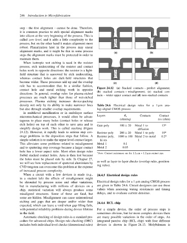
contact hole and metal etching work in opposite Figure 24.12 (a) Stacked contacts – perfect alignment;
(b) stacked contacts – misalignment; (c) stacked con-
directions. In general, overlap rules for plasma-etched tacts – wider upper contact and (d) non-stacked contacts
processes are much tighter than those of wet-etched
processes. Plasma etching increases device-packing
density not only by its ability to make narrower lines Table 24.6 Electrical design rules for a 1 µm ana-
but also through smaller overlap requirements. log–digital CMOS process
In multilevel metallization or in multilayer surface
Layers Contacts Contact
micromechanical processes, it would often be advan- R s
(ohm/sq) res (ohm)
tageous to place many holes (contact holes or release
etch holes) on top of each other to save area and to Gate poly 100 ± 20 Metal 1 to 15*
simplify design work. This is called stacking (Figure diffusion
24.12). However, it rapidly leads to serious step cov- Resistor poly 200 ± 20 Metal 1 to poly 10*
erage problems in the deposition steps that follow. A Resistor poly, 1000 ± 100 Metal 2 to metal 0.2*
simple solution is to make the upper-level contact larger. hi res 1
This alleviates some problems related to misalignment Metal 1 0.1
and to sputtering step coverage because a larger contact Metal 2 0.03
hole has a lower aspect ratio. Most often design rules ∗ Note: Contact resistances are for 1.2 µm × 1.2 µm contact size.
forbid stacked contact holes. Area is then lost because
the holes must be placed side by side. In Chapter 27,
we will see how replacement of sputtered aluminium by as well as layer-to-layer checks (overlap rules, position-
CVD tungsten can overcome this problem at the expense ing rules).
of increased process complexity.
When a circuit with a few devices is made (e.g., 24.4.5 Electrical design rules
in a student lab) the effects of misalignment might
be shrouded by process noise and other variations, Electrical design rules for a 1 µm analog CMOS process
but in manufacturing with millions of devices on a are given in Table 24.6. Circuit designers can use these
chip, statistical variation will always produce some values when assessing wiring resistances and timing
misaligned structures. Some of these are fatal, but delays, and to evaluate current densities.
some are hidden. Misalignment can cause unintentional
etching and gaps that are deeper and/or wider than
24.4.6 RCL chip
expected, which can leave a void when gap filling fails,
with potential reliability problems during device lifetime For a simple device, the order of process steps is
in the field. sometimes obvious, but for more complex devices there
Automatic checking of design rules is a standard pro- are many possible variations in the order of steps. An
cedure for advanced chips. Design rule checking (DRC) integrated passive chip (RCL chip) with four different
includes both individual level checks (dimensional rules) devices is shown in Figure 24.13. Molybdenum is