
Page 270 - Sami Franssila Introduction to Microfabrication
P. 270
Process Integration 249
has a higher dielectric constant and better electrical between silicon and oxide can seriously deplete the
quality than pure oxides. Films such as this are known interface of dopants, but this segregation is dependent
as NO, ONO and RONO, or nitrided oxide, oxidized on annealing/oxidation atmosphere: wet oxidation, dry
nitrided oxide and reoxidized nitrided oxide, respec- oxidation, inert anneal in nitrogen or reducing anneal in
tively. These films are standard CMOS gate dielectrics hydrogen rich ambient can behave differently.
in deep sub-micron technologies where oxide thickness Ion implantation annealing has two different ele-
is below 10 nm. ments: activation of dopants and damage removal. Acti-
The unintentional surface modification most com- vation energies for these processes are different, and
monly encountered is oxidation: some residual oxygen depending on the temperature, damage removal can
or moisture in a furnace atmosphere will lead to oxida- either be accomplished in a few seconds or it can take
tion. Copper annealing in a moist atmosphere will result hours. Transient enhanced diffusion has major impli-
in copper oxide, and 5 ppm water vapour is enough to cation for diffusion profiles, as will be discussed in
disturb titanium silicide formation. Oxidation is some- connection of shallow junctions in Chapter 25.
times done to protect the surface: for example, alu-
minium oxide is chemically much more stable than alu-
minium, and it is preferable to oxidize the aluminium 24.8 METALLIZATION
surface. Room temperature plasma oxidation (i.e., RIE
etching step with oxygen) will do the job. All electrical devices need at least one level of
metallization in order to connect to the outside world and
so do most mechanical, thermal, fluidic and bio-devices,
24.7 THERMAL BUDGET because electrical sensing and actuation are widely used.
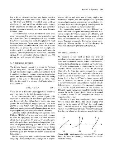
Metal to semiconductor contacts come in two basic
The thermal budget concept is a central to front-end
varieties: ohmic (resistive) or diode-like (Schottky)
process integration. Diffusion of dopants takes place in
all high-temperature steps: in addition to diffusion itself, (Figure 24.14). Even the ohmic contacts have some
it manifests itself during epitaxy, oxidation, densification diode character because metal and semiconductor work
anneal and implant damage annealing. The final doping functions are never exactly equal. If the semiconductor
3
19
profile is the sum of diffusion in all these steps. doping level is low (<10 /cm ), charge carriers will
Effective Dt, which is a measure of diffusion distance, have to overcome the barrier (which is proportional
is calculated as to metal workfunction–semiconductor electron affinity
difference ϕ metal − χ semiconductor ) by thermionic emission.
(Dt) eff = D n t n (24.1) In a heavily doped semiconductor, the situation is
different: charge carriers can tunnel through the barrier
where Ds are diffusivities under appropriate conditions because the barrier is thin. Barrier thickness is related
and ts are times for the high-temperature steps. to depletion width in the semiconductor (which is
In an aluminum gate CMOS process (Figure 19.1), proportional to 1/N D ).
source/drain diffusions are done before gate oxidation, Aluminium is the most widely-used ohmic contact
and dopants will, thus, diffuse further during gate oxide between metal and silicon. The silicon doping level
growth. In a self-aligned polygate process, gate oxide needs to be in excess of 10 /cm for good ohmic
19
3
growth is done before S/D formation, and therefore contact. Aluminium, which is a p-type dopant for silicon,
shallower junctions are possible because there are fewer can also be used to make an ohmic contact with a lightly
high-temperature steps after source/drain formation. doped p-type silicon: during contact anneal (in forming
A thermal budget sets limits on possible process steps.
PSG and BPSG film flow was once a standard technique
to make the topography smoother in CMOS processes
above 1 µm generations. Of course, it was only appli-
cable after polysilicon, not after metal deposition. How-
◦
ever, the required annealing (ca. 950–1000 C, depen-
dent on boron and phosphorous content) causes dopant
diffusion, and as junction depths were scaled down with
linewidth, glass flow became non-usable in sub-micron (a) (b) (c)
technologies. Figure 24.14 Metal-semiconductor contact I-V-curves (a)
Dopant segregation must be taken into account when ohmic; (b) diode-like (Schottky) and (c) real metal-semi-
designing a fabrication process. Segregation of dopants conductor contact