
Page 271 - Sami Franssila Introduction to Microfabrication
P. 271
250 Introduction to Microfabrication
◦
gas at 450 C), aluminium will dope the top surface of it is far from ideal. The interface-trapped charges are
the silicon and good contact is made. Schottky contacts caused by broken bonds (from structural defects, oxida-
to silicon are usually made with PtSi. tion induced defects and contamination). Because they
Contact resistance R c is given by are at the interface, the potential in silicon will charge
or discharge them. An interface-trapped charge can be
R c = ρ c /WL (24.2) reduced by forming gas anneal. There is always some
positive fixed charge in the vicinity of the interface, and
where ρ c is the contact resistivity, and W and L are the it is related to silicon ionization during the oxidation
contact dimensions. process. There are also trapped charges, which can be
Contact resistivity depends on barrier height (0.55 eV
positive or negative, caused by energetic electrons from
half bandgap of silicon) and silicon doping concentra- ionizing radiation, and there can be mobile charges from
20
3
tion (2 × 10 /cm maximum dopant solubility), which
contamination, most notably Na ions.
+
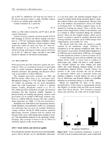
cannot be changed. Therefore, metal-to-silicon contact The electric field that oxide can sustain is usually
2
resistivities cannot be much less than 10 −7 ohm-cm .
reported by the breakdown voltage: 10 MV/cm is
This translates to ca. 0.1 ohm for 1 × 1 µm contacts.
considered to be the intrinsic breakdown field. This is
Metal-to-silicide and metal-to-metal contact resistivities also termed C-mode failure. B-mode failures happen at 2
2
are in the 10 −8 ohm-cm range, and this is one added to 8 MV/cm and A-mode below 2 MV/cm. An example
benefit of silicides in sub-micron technologies.
of oxide breakdown statistics is shown in Figure 24.15.
A-mode failures are gross defects: pinholes and voids
(Figure 24.16). COPs in silicon lead to oxidation of
24.9 RELIABILITY
microscopic pits, which will lead to oxide integrity
Final passivation provides protection against the envi- loss. B-mode failures are more benign and more
ronment. There are mechanical elements of passivation subtle, like oxide thinning, trapped charges or metal
such as scratch resistance, chemical aspects such as contamination induced defects. C-mode failures are
moisture resistance and gettering and physical effects intrinsic to the oxide structure, but can be affected
such as prevention of sodium diffusion. by nanoscopic defects such as increased surface and
The standard passivation materials are PSG and interface roughness. A-mode failures are seen as yield
PECVD nitride, either alone or as a two-layer stack. loss in fabrication and B-mode failures as reliability
Phosphorous doping of a CVD oxide film is beneficial problems in accelerated testing or in the field.
for sodium ion gettering, but too much phosphorus Metals are responsible for many of the defects
makes the oxide hygroscopic, so there is a delicate described above. If the surface is contaminated, silicates
balance. Usually, phosphorus content is ca. 5% wt. like MgSiO 4 or silicides CuSi and NiSi can be formed,
The nitride provides mechanical strength and chemical rather than silicon dioxide. Their formation consumes
resistance, but this chemical stability translates to silicon and, therefore, the oxide will be locally thinner.
plasma etching for bonding pad opening, whereas oxide
passivation can be etched in HF-based solutions (not,
however, without difficulty because HF-water solutions
attack aluminum: see Table 11.3 for etch selectivities).
Reliability has both built-in and operational features. C
Oxide thickness non-uniformity results in a permanent
non-uniformity that may pose, for example, breakdown
voltage variation. During the MOS transistor operation Breakdown frequency
high-energy electrons, scattered from the channel into
the gate oxide, cause oxide charge there, leading to wear- A B
out. This degradation depends on the operating voltage.
Similarly, step coverage is frozen in but its effects on
reliability depend on the current density.
1 5 10
24.9.1 Oxide defects and electrical quality
Breakdown field MV/cm
Even though the interface between silicon and thermally- Figure 24.15 Oxide breakdown distribution: A-mode at
grown silicon dioxide can be reproducibly fabricated, low field; B-mode at medium field and C-mode at high field