
Page 273 - Sami Franssila Introduction to Microfabrication
P. 273
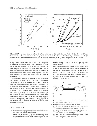
252 Introduction to Microfabrication


                       6
                                6
                          1.0 × 10  A/cm 2
                       3   AI(2%Cu)                        80                   0.36 MA/cm 2
                      10 2  AI(0.5%Cu)                             0.55 MA/cm 2
                           Pure Al
                       4                                   60
                       2                                      0.74 MA/cm 2
                    t (h)  8                             ∆ R (Ω)  40
                       3
                      10 0                                 20                     0.3 MA/cm 2

                       6
                       2                                   0
                                                                     W/Ti/AI(2%Cu)/Ti  Line-W stud
                     10 −1
                        14     17     20     23     26         0  200  400  600  800  1000 1200
                                          −1
                                       −4
                                  1/T (10  K )                            Time (h)
                                      (a)                                   (b)
            Figure 24.17 (a) mean time to failure of 2.5 µm wide Al, Al (0.5 wt% Cu) and Al(2 wt% Cu) lines at different
                                 2
            temperatures with 1 MA/cm current density. Reproduced from Hu, C.-K. et al. (1993), by permission of AIP. (b)
            incubation time before resistance increase sets in at 255 C. From Hu, C.-K. (1995a), by permission of Elsevier
                                                     ◦
                          ◦
            change when 300 C PECVD is done. This elongation  Include design features such as spacing rules
            corresponds to stresses over 1 GPa (the order of mag-  and dogbones.
            nitude can be estimated by Equation 4.1). Aluminium  3. Create a fabrication process for the platinum silicide
            lines expand during PECVD, and they are fixed at  Schottky diode shown below. Platinum silicide is
            their elongated state because of mechanical stiffness of  formed by metal/silicon reaction, not by etching.
            deposited oxide/nitride layers. This high tensile stress  From Chen, C.K. et al: Ultraviolet, visible and
            can be relaxed by cracks, and once a crack is formed, it  infrared response of PtSi Schottky-barrier detectors
            tends to grow.                                  operated in the front-illuminated mode, IEEE TED,
              Compressive stresses in aluminium can be relaxed  38 (1991) 1094, fig. 2.
            via hillock formation. Hillocks are small protrusions.
            Their size can be up to micrometres, which is equal to    Al
            insulator thickness between two levels of metallization.         PtSi      SiO 2
            If some mechanically stiffer film prevents relaxation in
            the vertical direction, then hillocks can grow laterally,
            and again, a micrometre is a very typical size for metal  p +  n       n      p +
            line spacing. In both cases, hillocks can short-circuit         p
            the two metal lines. Low-temperature processing helps   Si
            in reducing hillocks (and stress and electromigration).
            Alloying aluminium with copper is also helpful in
            minimizing hillock formation because it blocks grain  4. How do diffused resistor design rules differ from
            boundary diffusion.                             the thin-film resistor case?
                                                          5. Integrated passive chip (Figure 24.13):
            24.10 EXERCISES                                 (a) What is the nitride thickness if areal capacitance
                                                                             2
                                                               density is 4 nF/mm , and nitride ε r = 7?
             1. How many lithography steps are needed to fabricate  (b) Why is the first contact etching by plasma and
                the solar cell shown in Figure 1.6?            the second by wet etching?
             2. Draw the photomasks (e.g., on transparency film)  (c) SiCr thin-film resistor resistivity is 2000 µohm-
                required to fabricate the RCL chip of Figure 24.13.  cm. Design a 5 kohm resistor.