
Page 277 - Sami Franssila Introduction to Microfabrication
P. 277
256 Introduction to Microfabrication
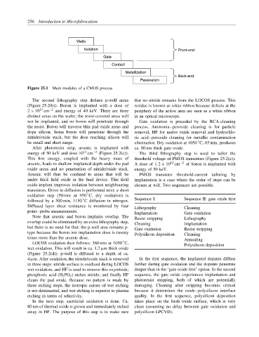
Wells
Isolation Front-end
Gate
Contact
Metallization
Back-end
Passivation
Figure 25.1 Main modules of a CMOS process
The second lithography step defines p-well areas that no nitride remains from the LOCOS process. This
(Figure 25.2(b)). Boron is implanted with a dose of residue is known as white ribbon because defects at the
13
2 × 10 cm −2 and energy of 40 keV. There are three periphery of the active area are seen as a white ribbon
distinct areas on the wafer; the resist-covered areas will in an optical microscope.
not be implanted, and no boron will penetrate through Gate oxidation is preceded by the RCA-cleaning
the resist. Boron will traverse thin pad oxide areas and process. Ammonia–peroxide cleaning is for particle
dope silicon. Some boron will penetrate through the removal, HF for native oxide removal and hydrochlo-
nitride/oxide stack, but the dose reaching silicon will ric acid–peroxide cleaning for metallic contamination
be small and short range. elimination. Dry oxidation at 1050 C, 65 min, produces
◦
After photoresist strip, arsenic is implanted with ca. 80 nm thick gate oxide.
12
energy of 50 keV and dose 10 cm −2 (Figure 25.2(c)). The third lithography step is used to tailor the
This low energy, coupled with the heavy mass of threshold voltage of PMOS transistors (Figure 25.2(e)).
arsenic, leads to shallow implanted depth under the pad A dose of 1.2 × 10 cm −2 of boron is implanted with
12
oxide areas and no penetration of nitride/oxide stack. energy of 50 keV.
Arsenic will thus be confined to areas that will be PMOS transistor threshold-current tailoring by
under thick field oxide in the final device. This field implantation is a case where the order of steps can be
oxide implant improves isolation between neighbouring chosen at will. Two sequences are possible.
transistors. Drive-in diffusion is performed next: a short
oxidation step (50 min at 950 C, dry oxidation) is
◦
◦
followed by a 500 min, 1150 C diffusion in nitrogen. Sequence I: Sequence II: gate oxide first
Diffused layer sheet resistance is monitored by four Lithography Cleaning
point–probe measurements.
Implantation Gate oxidation
Note that arsenic and boron implants overlap. The
Resist stripping Lithography
overlap could be eliminated by an extra lithography step,
Cleaning Implantation
but there is no need for that: the p-well area remains p-
Gate oxidation Resist stripping
type because the boron ion implantation dose is twenty Polysilicon deposition Cleaning
times more than the arsenic dose. Annealing
◦
LOCOS oxidation then follows: 360 min at 1050 C, Polysilicon deposition
wet oxidation. This will result in ca. 1.2 µm thick oxide
(Figure 25.2(d)). p-well is diffused to a depth of ca.
4 µm. After oxidation, the nitride/oxide stack is removed In the first sequence, the implanted dopants diffuse
in three steps: nitride surface is oxidized during LOCOS further during gate oxidation and the dopants penetrate
wet oxidation, and HF is used to remove this oxynitride; deeper than in the ‘gate oxide first’ option. In the second
phosphoric acid (H 3 PO 4 ) etches nitride; and finally HF sequence, the gate oxide experiences implantation and
clears the pad oxide. Because no pattern is made by photoresist stripping, both of which are potentially
these etching steps, the isotropic nature of wet etching damaging. Cleaning after stripping becomes critical
is not detrimental, and wet etching is superior to plasma because it determines the oxide–polysilicon interface
etching in terms of selectivity. quality. In the first sequence, polysilicon deposition
In the next step, sacrificial oxidation is done. Ca. takes place on the fresh oxide surface, which is very
80 nm of thermal oxide is grown and immediately etched clean (assuming no delay between gate oxidation and
away in HF. The purpose of this step is to make sure polysilicon LPCVD).