
Page 281 - Sami Franssila Introduction to Microfabrication
P. 281
260 Introduction to Microfabrication
Table 25.4 Front-end scaling (ca. 1980–1995): supply
voltage constant at 5 V
Generation 3 µm 2 µm 1.5 µm 1 µm 0.7 µm 0.5 µm Oxide growth Ion implantation dose
conditions and energy
T ox (nm) 70 40 30 25 20 14
x j (nm) 600 400 300 250 200 150
Gate delay 800 350 250 200 160 90 Process simulator
(ps)
Doping profiles Optimize
Table 25.5 CMOS front-end scaling at the turn of the
millenium
Device simulator
Generation 0.35 µm 0.25 µm 0.18 µm 0.13 µm
T ox (nm) 8 6 4.5 4
Supply (V) 3.3 2.5 1.8 1.5 Device performance,
V th (V) 0.65 0.6 0.5 0.45
I off vs. V th
Figure 25.3 Front-end process development loop depends
′
which necessitates lower operating voltage, V , given by heavily on process simulation
V = V/n (Table 25.5). Using shorthand V ≡ V gs − V th ,
′
we can write the physical parameters for the scaled 25.3 ADVANCED CMOS ISSUES
devices as shown in Table 25.3.
The 5 µm CMOS process presented above has main
Scaling is mostly beneficial: transistor area scales as features similar to any modern CMOS process. Over
2
2
2
′
′
′
1/n (A = L W = LW /n = A/n ), transistor speed the years, refinements, modifications, materials changes
2
increases as 1/n, switching power decreases as 1/n and and many other improvements have taken place. The
3
switching energy decreases as 1/n . The power density
CMOS process of the year 2000 with 0.25 µm linewidth
(P/A) remains constant. Junction depth scaling, x j , has
and over 25 mask levels is quite advanced compared to
been mostly in line with oxide thickness scaling, but
9 mask levels for 5 µm. We will not discuss changes
more recently it has been difficult to keep the pace.
generation by generation, but rather look at some
This is because ion implantation damage necessitates
important trends in processes and structures themselves.
high-temperature annealing, which inevitably leads to
At and below 1 µm, the following features have been
diffusion however shallow the original implantation
implemented in CMOS:
profile. Linewidth scaling is just one factor in packing
density increase: process and device cleverness can – step-and-repeat 5X reduction lithography with λ =
contribute amazingly large area reductions. 365 nm;
Note that gate oxide thickness is related to linewidth – spacers and LDD implants;
L roughly as L/45 and junction depth is ca. L/5. – silicides;
– CVD-W plugs;
– planarization.
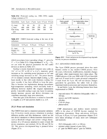
25.2.3 Front end simulation
CMP planarization and shallow trench isolation
The CMOS front end is a transistor parameter optimiza- (STI) in the place of LOCOS become standard for
tion. It involves mostly process simulation to produce half-micron generations. Deep sub-micron (0.35 µm,
diffusion profiles and film thicknesses, which are fed 0.25 µm, 0.18 µm, 0.13 µm) generations (Figure 25.4)
into device simulators to obtain transistor characteristics have taken advantage of many more new techniques
such as threshold voltages and current–voltage charac- and materials:
teristics. If a 1D process simulator is used, it feeds 1D
device simulation, and similarly 2D for 2D and 3D for – DUV-lithography with λ = 248 nm;
3D. This process development loop is pictured below – nitrided oxides instead of pure SiO 2 ;
+
(Figure 25.3). – p gate for PMOS and n gate for NMOS;
+