
Page 283 - Sami Franssila Introduction to Microfabrication
P. 283
262 Introduction to Microfabrication
(a) (b)
(c) (d)
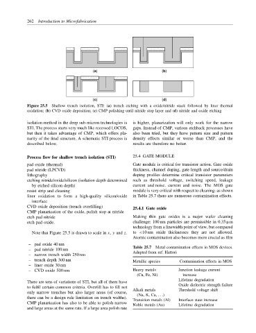
Figure 25.5 Shallow trench isolation, STI: (a) trench etching with a oxide/nitride stack followed by liner thermal
oxidation; (b) CVD oxide deposition; (c) CMP polishing until nitride stop layer and (d) nitride and oxide etching
isolation method in the deep sub-micron technologies is is higher, planarization will only work for the narrow
STI. The process starts very much like recessed LOCOS, gaps. Instead of CMP, various etchback processes have
but then it takes advantage of CMP, which offers pla- also been tried, but they have pattern size and pattern
narity of the final structure. A schematic STI process is density effects similar or worse than CMP, and the
described below. results are therefore no better.
Process flow for shallow trench isolation (STI) 25.4 GATE MODULE
pad oxide (thermal) Gate module is critical for transistor action. Gate oxide
pad nitride (LPCVD) thickness, channel doping, gate length and source/drain
lithography doping profiles determine critical transistor parameters
etching nitride/oxide/silicon (isolation depth determined such as threshold voltage, switching speed, leakage
by etched silicon depth) current and noise. current and noise. The MOS gate
resist strip and cleaning module is very critical with respect to cleaning: as shown
liner oxidation to form a high-quality silicon/oxide in Table 25.7 there are numerous contamination effects.
interface
CVD oxide deposition (trench overfilling) 25.4.1 Gate oxide
CMP planarization of the oxide, polish stop at nitride
etch pad nitride Making thin gate oxides is a major wafer cleaning
etch pad oxide. challenge: 100 nm particles are permissible in 0.35 µm
technology from a linewidth point of view, but compared
Note that Figure 25.5 is drawn to scale in x, y and z. to <10 nm oxide thicknesses they are not allowed.
Atomic contamination also becomes more crucial as film
– pad oxide 40 nm
– pad nitride 100 nm Table 25.7 Metal contamination effects in MOS devices.
Adapted from ref. Hattori
– narrow trench width 250 nm
– trench depth 300 nm Metallic species Contamination effects in MOS
– liner oxide 30 nm
– CVD oxide 500 nm Heavy metals Junction leakage current
(Cu, Fe, Ni) increase
Lifetime degradation
There are tens of variations of STI, but all of them have
Oxide dielectric strength failure
to fulfil certain common criteria. Overfill has to fill not
Alkali metals Threshold voltage shift
only narrow trenches but also larger areas (of course,
(Na, K, Ca, . . .)
there can be a design rule limitation on trench widths).
Transition metals (Al) Interface state increase
CMP planarization has also to be able to polish narrow Noble metals (Au) Lifetime degradation
and large areas at the same rate. If a large area polish rate