
Page 286 - Sami Franssila Introduction to Microfabrication
P. 286
CMOS Transistor Fabrication 265
diffusion under normal low concentration conditions, deposited, and the final metal gate is deposited (followed
the activation energy is 3.66 eV, but in ion implanted, by CMP). The replacement gate makes the return of
damaged silicon it is 2.2 eV. Because rate is expo- the aluminium gate possible, but refractory metals are
nentially related to activation energy (Equation 1.1), more likely candidates. The added process complexity is
dramatic changes in phosphorus diffusion take place. quite big, and oxidation/oxide deposition into the groove
Point defects, interstitials and vacancies, created during left by dummy gate etching is by no means easy or
implantation, offer fast diffusion paths. This is known straightforward.
as transient enhanced diffusion (TED). If defects can
be annealed away rapidly, TED is eliminated and ther-
mal diffusion determines doping profiles. Elimination 25.5 CONTACT TO SILICON
of extended defects, such as dislocation loops, requires Scaling of contact size has rapidly led to problems
◦
1050 C anneals. with contact resistance. Contact resistance is given by
Rapid thermal annealing (RTA) is a solution to Equation 24.1. If 0.4 µm contacts are made only at the
this problem. A short time, high-temperature step bottom of the contact hole, resistance will be 10 −7 ohm-
◦
(e.g., 1–10 s, 1000–1100 C) is used to anneal implant cm /(0.4 µm) = 63 ohm, compared with 16 ohm for
2
2
damage. Thermal diffusion will be insignificant because 0.8 µm contacts. If, however, the whole source/drain
the time is very short. Another anneal, at lower area (1 µm ×1 µm) is silicided, silicon-to-silicide con-
temperature but in longer time, will thermally diffuse tact resistance will be 10 −7 ohm-cm /1 × 10 −8 cm =
2
.
2
dopants and activate them. RTA will be further discussed 10 ohm. Metal-to-silicide contact area is 0.4 × 0.4 µm ,
2
in Chapter 31.
so that will contribute only 1.25 ohm. Total contact resis-
tance is thus only 11.25 ohm, compared with 63 ohm for
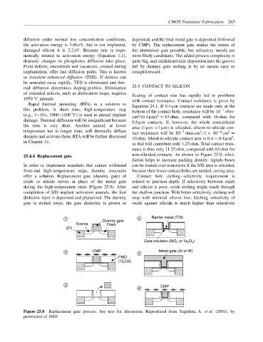
25.4.4 Replacement gate non-silicided contacts. As shown in Figure 25.9, silici-
dation helps to increase packing density: signals buses
In order to implement materials that cannot withstand can be routed over transistors if the S/D area is silicided,
front-end high-temperature steps, dummy structures because then fewer contact holes are needed, saving area.
offer a solution. Replacement gate (dummy gate) of Contact hole etching–selectivity requirement is
oxide or nitride serves in place of the metal gate related to junction depth. If selectivity between oxide
during the high-temperature steps (Figure 25.8). After and silicon is poor, oxide etching might reach through
completion of S/D implant activation anneals, the first the shallow junction. With better selectivity, etching will
dielectric layer is deposited and planarized. The dummy stop with minimal silicon loss. Etching selectivity of
gate is etched away, the gate dielectric is grown or oxide against silicide is much higher than selectivity
1 Dummy gate 4 Barrier metal (TiN)
Source Drain
STI
Gate insulator (SiO 2 or Ta 2 O 5 )
2 CMP 5 Metal gate (AI or W)
PMD
(TEOS)
3 CMP
6
Figure 25.8 Replacement gate process. See text for discussion. Reproduced from Yagishita, A. et al. (2001), by
permission of IEEE