
Page 282 - Sami Franssila Introduction to Microfabrication
P. 282
CMOS Transistor Fabrication 261
+
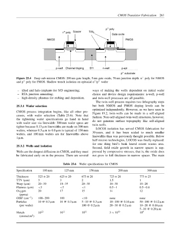
p poly
+
n poly Spacer TiSi 2
Gate oxide
NMOS PMOS
p-well Channel doping STI n-well p-epi
+
p substrate
+
Figure 25.4 Deep sub-micron CMOS: 200 nm gate length, 5 nm gate oxide, 70 nm junction depth. n poly for NMOS
+
+
+
and p poly for PMOS. Shallow trench isolation on epitaxial n /p wafer
– tilted and halo implants for S/D engineering; ways of making the wells dependent on initial wafer
– RTA junction annealing; choice and device design requirements: n-well, p-well
– high-density plasmas for etching and deposition. and twin-well processes are all possible.
The twin-well process requires two lithography steps
25.3.1 Wafer selection but both NMOS and PMOS doping levels can be
optimized independently. However, as we have seen in
CMOS process integration begins, like all other pro- Figure 19.2, twin-wells can be made in a self-aligned
cesses, with wafer selection (Table 25.6). Note that fashion. Non-self-aligned twin-well structures, however,
the tightening wafer specifications go hand in hand do not generate surface topography like self-aligned
with wafer size via linewidth: 300 mm wafer specs are twin-wells.
tighter because 0.13 µm linewidths are made on 300 mm
wafers, whereas 0.5 µm to 0.8 µm is typical of 150 mm LOCOS isolation has served CMOS fabrication for
wafers, and 100 mm wafers are for linewidths above 30 years, and it has been scaled to much smaller
1 µm. linewidths than was previously thought possible. Below
half-micron technologies, LOCOS was finally replaced:
for one thing bird’s beak lateral extent wastes area.
25.3.2 Wells and isolation
Second, field oxide growth in narrow spaces is sup-
Wells are the deepest diffusions in CMOS, and they must pressed by compressive stresses, that is, the oxide does
be fabricated early on in the process. There are several not grow to full thickness in narrow spaces. The main
Table 25.6 Wafer specifications for CMOS
Specification 100 mm 125 mm 150 mm 200 mm 300 mm
Thickness 525 ± 20 625 ± 20 675 ± 20 725 ± 20 775 ± 25
TTV (µm) 3 3 2 1.5 1
Warp (µm) 20–30 18–35 20–30 10–30 10–20
Flatness (µm) <3 <2 <1 0.5−1 0.5−0.8
Oxygen 20 17 15 14 12
(ppma)
−2
OISF (cm ) 100–200 100 <10 none none
Particles 10 @ 0.3 µm 10 @ 0.3 µm 5–10 @ 0.3 µm 10–100 @ 0.16 µm 50–100 @ 0.12 µm
(per wafer) 100 @ 0.2 µm 20–30 @ 0.2 µm 10–20 @ 0.16 µm
5–10 @ 0.20 µm
Metals 10 12 10 11 10 11 5 × 10 10 10 9
2
(atoms/cm )