
Page 285 - Sami Franssila Introduction to Microfabrication
P. 285
264 Introduction to Microfabrication
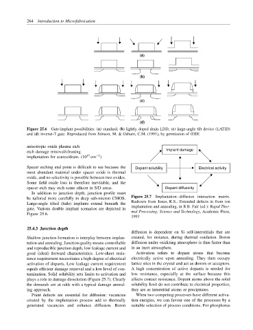
(a)
(b)
(c)
(d)
Figure 25.6 Gate-implant possibilities: (a) standard; (b) lightly doped drain LDD; (c) large-angle tilt device (LATID)
and (d) inverse-T gate. Reproduced from Stinson, M. & Osburn, C.M. (1991), by permission of IEEE
anisotropic oxide plasma etch
etch damage removal/cleaning Implant damage
−2
15
implantation for source/drain. (10 cm )
Spacer etching end point is difficult to see because the Dopant solubility Electrical activity
most abundant material under spacer oxide is thermal
oxide, and no selectivity is possible between two oxides.
Some field oxide loss is therefore inevitable, and the
spacer etch may etch some silicon in S/D areas. Dopant diffusivity
In addition to junction depth, junction profile must
Figure 25.7 Implantation–diffusion interaction matrix.
be tailored more carefully in deep sub-micron CMOS.
Redrawn from Jones, K.S., Extended defects in from ion
Large-angle tilted (halo) implants extend beneath the
gate. Various double implant scenarios are depicted in implantation and annealing, in R.B. Fair (ed.): Rapid Ther-
Figure 25.6. mal Processing: Science and Technology, Academic Press,
1993
25.4.3 Junction depth
diffusion is dependent on Si self-interstitials that are
Shallow junction formation is interplay between implan- created, for instance, during thermal oxidation. Boron
tation and annealing. Junction quality means controllable diffusion under oxidizing atmosphere is thus faster than
and reproducible junction depth, low leakage current and in an inert atmosphere.
good (ideal) forward characteristics. Low-sheet resis- Activation refers to dopant atoms that become
tance requirement necessitates a high degree of electrical electrically active upon annealing. They then occupy
activation of dopants. Low leakage current requirement lattice sites in the crystal and act as donors or acceptors.
equals efficient damage removal and a low level of con- A high concentration of active dopants is needed for
tamination. Solid solubility sets limits to activation and low resistance, especially at the surface because this
plays a role in damage dissolution (Figure 25.7). Clearly affects contact resistance. Dopant atoms above the solid
the demands are at odds with a typical damage anneal- solubility limit do not contribute to electrical properties;
ing approach. they are as interstitial atoms or precipitates.
Point defects are essential for diffusion: vacancies When two competing processes have different activa-
created by the implantation process add to thermally tion energies, we can favour one of the processes by a
generated vacancies and enhance diffusion. Boron suitable selection of process conditions. For phosphorus