
Page 288 - Sami Franssila Introduction to Microfabrication
P. 288
CMOS Transistor Fabrication 267
Jones, K.S., Extended defects in from ion implantation and
annealing, in R.B. Fair (ed.): Rapid Thermal Processing:
Science and Technology, Academic Press, 1993.
Hori, T. & Sugano, T. (eds.): Gate Dielectrics and MOS
ULSIs: Principles, Technologies and Applications, Springer,
1997.
Kahng, D.: A historical perspective on the development of
MOS transistors and related devices, IEEE TED, 23 (1976),
655.
Liu, R., Metallization, in C.Y. Chang & S.M. Sze (eds.): ULSI
Technology, McGraw-Hill, 1996, p. 400.
Saitoh, W. et al: 35 nm metal gate p-type metal oxide semicon-
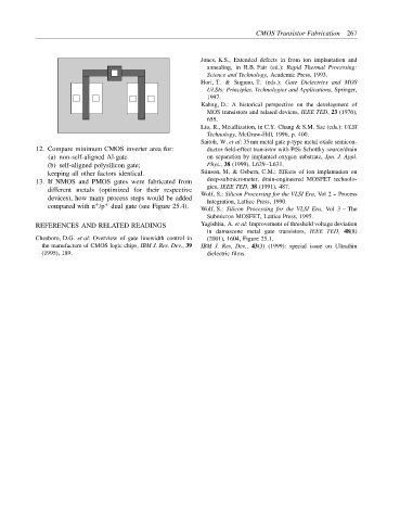
12. Compare minimum CMOS inverter area for: ductor field-effect transistor with PtSi Schottky source/drain
(a) non-self-aligned Al-gate on separation by implanted oxygen substrate, Jpn. J. Appl.
(b) self-aligned polysilicon gate; Phys., 38 (1999), L629–L631.
keeping all other factors identical. Stinson, M. & Osburn, C.M.: Effects of ion implantation on
13. If NMOS and PMOS gates were fabricated from deep-submicrometer, drain-engineered MOSFET technolo-
gies, IEEE TED, 38 (1991), 487.
different metals (optimized for their respective Wolf, S.: Silicon Processing for the VLSI Era, Vol 2 – Process
devices), how many process steps would be added Integration, Lattice Press, 1990.
+
+
compared with n /p dual gate (see Figure 25.4).
Wolf, S.: Silicon Processing for the VLSI Era, Vol 3 – The
Submicron MOSFET, Lattice Press, 1995.
REFERENCES AND RELATED READINGS Yagishita, A. et al: Improvement of threshold voltage deviation
in damascene metal gate transistors, IEEE TED, 48(8)
Chesboro, D.G. et al: Overview of gate linewidth control in (2001), 1604, Figure 25.1.
the manufacture of CMOS logic chips, IBM J. Res. Dev., 39 IBM J. Res. Dev., 43(3) (1999): special issue on Ultrathin
(1995), 189. dielectric films.