
Page 293 - Sami Franssila Introduction to Microfabrication
P. 293
272 Introduction to Microfabrication
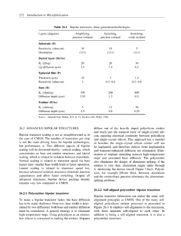
Table 26.1 Bipolar transistors, three generations/technologies
Layers (dopants) Amplifying, Switching, Switching,
junction isolated junction isolated oxide isolated
Substrate (B)
Resistivity (ohm-cm) 10 10 5
Orientation (111) (111) (111)
Buried layer (Sb/As)
R s ( /sq) 20 20 30
Up-diffusion (µm) 2.5 1.4 0.3
Epitaxial film (P)
Thickness (µm) 10 3 1.2
Resistivity (ohm-cm) 1 0.3–0.8 0.3–0.8
Base (B)
R s (ohm/sq) 100 200 600
Diffusion depth (µm) 3.25 1.3 0.5
Emitter (P/As)
R s (ohm/sq) 5 12 30
Diffusion depth (µm) 2.5 0.8 0.25
Source: Adapted from Muller, R.S. & T.I. Kamins John Wiley, 1986.
26.2 ADVANCED BIPOLAR STRUCTURES diffuse out of the heavily doped polysilicon emitter
and reach just the topmost layer of single-crystal sili-
Bipolar transistor scaling is not as straightforward as in con, ensuring electrical continuity between polysilicon
the case of CMOS. The number of transistors per chip and single-crystal silicon. This approach has a number
is not the main driving force for bipolar technologies, of benefits: the single-crystal silicon emitter will not
but performance is. Two different aspects of bipolar be implanted, and therefore defects from implantation
scaling will be discussed shortly: vertical scaling, which and transient-enhanced diffusion are eliminated. Elim-
concentrates on base and emitter structures; and lateral ination of implant annealing reduces high-temperature
scaling, which is related to isolation between transistors. steps and unwanted base diffusion. The polyemitter
Vertical scaling is related to transistor speed via base also eliminates the danger of aluminum spiking: if the
transit time: smaller base width leads to faster operation. emitter is very thin, aluminium might spike through
Lateral scaling is related to transistor speed too, it, destroying the device (recall Figure 7.6(e)). Polysil-
because advanced isolation structures eliminate junction icon, for example 200 nm thick, between aluminium
capacitances and allow faster switching. Despite all and the emitter/base junction eliminates the aluminium-
advanced structures, bipolar device packing density spiking problem.
remains very low compared to CMOS.
26.2.2 Self-aligned polyemitter bipolar transistor
26.2.1 Polyemitter bipolar transistor
Bipolar transistor fabrication can utilize the same self-
To make a bipolar transistor faster, the base diffusion alignment principles as CMOS. One of the many self-
has to be made shallower. However, base width is deter- aligned polysilicon emitter processes is presented in
mined by two diffusions: both base and emitter diffusion Figure 26.4. It employs self-alignment to the maximum,
must be considered. A general strategy is to eliminate with three implants self-aligned to each other. In
high-temperature steps. Using polysilicon as an emitter, addition to being a self-aligned transistor, it is also a
less silicon is consumed in making the emitter. Dopants polyemitter transistor.