
Page 296 - Sami Franssila Introduction to Microfabrication
P. 296
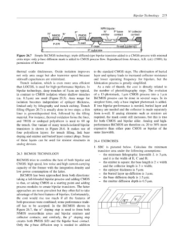
Bipolar Technology 275


                                                           NPN bipolar  +   +
                                                              +
                            N +      N +    P +     P +     N     P base   N collector
                               NMOS           PMOS         emitter  contact  contact
                               P-EPI          N-well
                                                     P-base         N-well (collector)
                                                   P substrate
                                                    +
           Figure 26.7 Simple BiCMOS technology: triple diffused-type bipolar transistor added to a CMOS-process with minimal
           extra steps: only p-base diffusion mask is added to CMOS process flow. Reproduced from Alvarez, A.R. (ed.) (1989), by
           permission of Kluwer

           thermal oxide thicknesses. Oxide isolation improves  to the standard CMOS steps. The elimination of buried
           not only area usage but also transistor speed because  layer and epitaxy leads to increased collector resistance
           sidewall capacitances are minimized.        and lower operating frequency for bipolars, but the
             Trench isolation, which is even more area efficient  fabrication process is greatly simplified.
           than LOCOS, is used for high-performance bipolars. In  As a rule of thumb, the cost is directly related to
           bipolar technology, deep trenches of 5 µm are typical,  the number of photolithography steps. The evolution
           in contrast to CMOS isolation where shallow trenches  of a 13-photomask, 1 µm CMOS process into a 1 µm
           (ca. 0.3 µm) are used (Figure 25.5). Area usage for  BiCMOS process can be done in several ways. In its
           isolation becomes independent of epilayer thickness,  simplest form, only a base implant photomask is added.
           limited only by lithography and trench etching. Trench  If true bipolar performance is needed, buried layer and
           filling (Figure 20.7) is usually done in two steps: a thin  epitaxy are needed and the collector is made separately
           liner is grown/deposited first, followed by the filling  from n-well. If analog elements such as resistors are
           material. For instance, thermal oxidation forms the liner,  required, the mask count still increases, but this is true
           and TEOS or undoped polysilicon is used to fill up  for both CMOS and bipolar alike. Analog and high-
           the trench. One variant of many trench-isolated bipolar  performance BiCMOS are therefore ca. 20 to 30% more
           transistors is shown in Figure 26.6. It makes use of  expensive than either pure CMOS or bipolar of the
           four polysilicon layers: for trench filling, link base  same linewidth.
           doping and emitter and buried layer contact plugs. Some
           of these layers can be used for resistor structures in  26.4 EXERCISES
           analog devices.
                                                       1. SBC is pictured below. Calculate the minimum
                                                         transistor area under the following assumptions:
           26.3 BiCMOS TECHNOLOGY                         – the minimum lithographic linewidth L is 3 µm,
                                                            and it is the width of E, C and B;
           BiCMOS tries to combine the best of both bipolar and
                                                          – the emitter is square; the base length is 2 × width
           CMOS: high speed, low noise and high current-carrying
                                                            and the collector length is 3 × width;
           capacity of the former with the integration density and
                                                          – the epilayer thickness is 5 µm;
           low power consumption of the latter.
             BiCMOS has been approached from both directions:  – the buried layer up-diffusion is 1 µm;
           taking a full-blooded bipolar process and adding CMOS  – the base diffusion depth is 1.5 µm;
           to that, or taking CMOS as a starting point and adding  – the emitter diffusion depth is 0.5 µm.
           process modules to create bipolar transistors. The latter
           approaches are more prevalent but they often fail to take
           advantage of the best features of bipolars. Unfortunately,
           the cost would rise too much if all the features of      C         B
           both processes were combined; some performance trade-        E
           off has to be accepted. In the BiCMOS shown in
           Figure 26.7, the n +  doping step is used to form both
           NMOS source/drain areas and bipolar emitters and
           collector contacts; and similarly, the p +  doping step
           creates both PMOS S/D and the bipolar base contact.
           Only the p-base diffusion step is needed in addition