
Page 292 - Sami Franssila Introduction to Microfabrication
P. 292
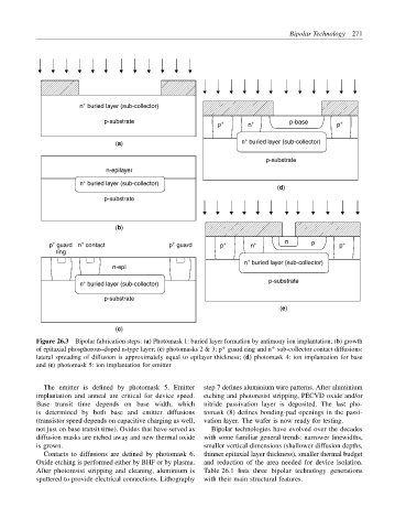
Bipolar Technology 271


                      n  buried layer (sub-collector)
                       +
                             p-substrate                   +       +         p-base        +
                                                          p       n                       p

                                                                  +
                                (a)                              n  buried layer (sub-collector)
                                                                       p-substrate
                             n-epilayer

                      n  buried layer (sub-collector)
                       +
                                                                          (d)
                             p-substrate


                               (b)
                                                                            n      p
               +
                                               +
                      +
              p  guard n  contact             p  guard     p +     n +                     p +
                ring
                                                                  +
                                                                 n  buried layer (sub-collector)
                               n-epi
                                                                        p-substrate
                       +
                      n  buried layer (sub-collector)
                             p-substrate
                                                                           (e)
                                (c)
           Figure 26.3 Bipolar fabrication steps: (a) Photomask 1: buried layer formation by antimony ion implantation; (b) growth
                                                            +
                                                                         +
           of epitaxial phosphorous-doped n-type layer; (c) photomasks 2 & 3: p guard ring and n sub-collector contact diffusions:
           lateral spreading of diffusion is approximately equal to epilayer thickness; (d) photomask 4: ion implantation for base
           and (e) photomask 5: ion implantation for emitter
             The emitter is defined by photomask 5. Emitter  step 7 defines aluminium wire patterns. After aluminium
           implantation and anneal are critical for device speed.  etching and photoresist stripping, PECVD oxide and/or
           Base transit time depends on base width, which  nitride passivation layer is deposited. The last pho-
           is determined by both base and emitter diffusions  tomask (8) defines bonding-pad openings in the passi-
           (transistor speed depends on capacitive charging as well,  vation layer. The wafer is now ready for testing.
           not just on base transit time). Oxides that have served as  Bipolar technologies have evolved over the decades
           diffusion masks are etched away and new thermal oxide  with some familiar general trends: narrower linewidths,
           is grown.                                   smaller vertical dimensions (shallower diffusion depths,
             Contacts to diffusions are defined by photomask 6.  thinner epitaxial layer thickness), smaller thermal budget
           Oxide etching is performed either by BHF or by plasma.  and reduction of the area needed for device isolation.
           After photoresist stripping and cleaning, aluminium is  Table 26.1 lists three bipolar technology generations
           sputtered to provide electrical connections. Lithography  with their main structural features.