
Page 295 - Sami Franssila Introduction to Microfabrication
P. 295
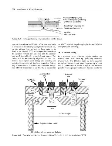
274 Introduction to Microfabrication


                                                              n  poly emitter (poly #2)
                                                               +
                                                              CVD oxide spacer (oxide #2)
                                                              CVD oxide (oxide #1)
                                                              Base link p poly (poly #1)
                                                                      +
                                                                             +
                                                              Base link diffusion (p )
                                                              n emitter
                                                              p intrinsic base

            Figure 26.5 Self-aligned double poly bipolar (see text for details)

                                                              ◦
            structure has to be etched. Etching of the base poly leads  ca. 950 C required for poly doping by thermal diffusion
            to some loss of the underlying single-crystal silicon too,  or implantation annealing.
            but the intrinsic base has not yet been made so its
            depth is not affected. CVD oxide deposition determines
                                                         26.2.4 Lateral scaling
            the distance between the link base and the intrinsic
            base non-lithographically, in a self-aligned manner. The  In a standard buried collector, bipolar devices are
            emitter will be automatically aligned to the base, too.  isolated from each other by guard-ring diffusions
            Intrinsic base implant dose, energy and annealing are  (Figure 26.1). The diffusion depth has to be equal to
            optimized irrespective of link base properties. Emitter  the epilayer thickness, and guard rings take up a lot of
            poly is doped in situ in order to reduce thermal budget:  area. LOCOS isolation, shown in Figure 26.3, becomes
                                         ◦
            poly LPCVD temperature is ca. 600 C, as against the  possible when epilayer thicknesses become similar to
                                       As-implanted            B-doped
                                          poly                   poly
                           1st AI wire                                      Tungsten
                                        B         E         B          C      plug


                             Oxide

                            Nitride
                                                                      n+
                                                                      Poly
                                   Oxide         SIC                  plug


                                                 1 µm

                                                           +
                                                          n  buried layer


                                       Polysilicon-filled trench


                              SIC = Selectively Ion-implanted Collector
            Figure 26.6 Trench isolated bipolar. Reproduced from Ugajin, M. (1995), by permission of IEEE