
Page 300 - Sami Franssila Introduction to Microfabrication
P. 300
Multilevel Metallization 279
1st interconnect
Goal (contact plug)
Silicon
Silicon
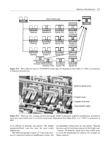
Cleaning Selective W Sputter TIN Sputter Al
Cleaning Sputter Tl Sputter TIN Sputter Al
Cleaning Sputter Tl Sputter TIN Blanket W
Etchback (W)
Etchback (TIN) Sputter TIN Sputter AI
Figure 27.4 Three different routes to Ti/TiN/W/Al contact plug fill. Reproduced from Ohba, T. (1992), by permission
of Materials Research Soc
Aluminum global wiring
Tungsten plugs
Tungsten local wires
TiSi 2 /polysilicon gates
Figure 27.5 Tilted top-view scanning electron micrograph (SEM) of planarized multilevel metallization: all dielectric
layers have been etched away to reveal the metal levels. Reproduced from Mann, R.W. et al. (1995), by permission of
IBM
to be difficult in principle and practice. The blanket top aluminium wiring levels are very planar. Tungsten
tungsten/etchback route has been the most widely has been used for local interconnects (in the length scale
adopted one. ∼10 µm). All dielectric layers have been etched away
The SEM micrograph of Figure 27.5 shows the struc- to reveal the metallization for analysis (for example for
ture of a planarized multilevel metallization scheme. The failure analysis).