
Page 303 - Sami Franssila Introduction to Microfabrication
P. 303
282 Introduction to Microfabrication
Si N 600
3 4
Polyimide Cu 500
Si N 400 Line width
2 µm
3 4
Polyimide Cu Ta Amount of dishing (nm) 300 5 µm
10 µm
50 µm
Si N 200 20 µm
3 4
CVD W
Oxide 100 µm
POLY 100 200 µm
ROX
0
n + Substrate n + 0 20 40 60 80 100
Pattern density (%)
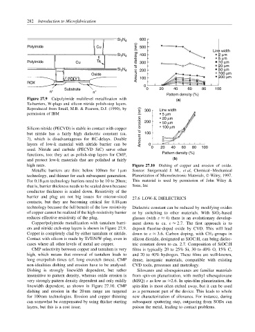
Figure 27.9 Cu/polyimide multilevel metallization with (a)
Ta-barriers, W-plugs and silicon nitride polish-stop layers.
Reproduced from Small, M.B. & Pearson, D.J. (1990), by 300 Line width
permission of IBM 5 µm
20 µm
100 µm
Silicon nitride (PECVD) is stable in contact with copper Amount of erosion (nm) 200 50 µm
but nitride has a fairly high dielectric constant (ca. 100
7), which is disadvantageous for RC-delays. Double
layers of low-k material with nitride barrier can be 0
used. Nitride and carbide (PECVD SiC) serve other 0 20 40 60 80 100
Pattern density (%)
functions, too: they act as polish-stop layers for CMP,
and protect low-k materials that are polished at fairly (b)
high rates. Figure 27.10 Dishing of copper and erosion of oxide.
Metallic barriers are thin: below 100nm for 1 µm Source: Steigerwald J. M., et al, Chemical–Mechanical
technology, and thinner for each subsequent generation. Planarization of Microelectronic Materials, Wiley, 1997.
For 0.18 µm technology barriers need to be 10 to 20nm; This material is used by permission of John Wiley &
that is, barrier thickness needs to be scaled down because Sons, Inc
conductor thickness is scaled down. Resistivity of the
barrier and plug are not big issues for micron-sized
27.6 LOW-K DIELECTRICS
contacts, but they are becoming critical for 0.18 µm
technology because the full benefit of the low resistivity Dielectric constant can be reduced by modifying oxides
of copper cannot be realized if the high-resistivity barrier or by switching to other materials. With SiO 2 -based
reduces effective resistivity of the plug. glasses (with ε ≈ 4) there is an evolutionary develop-
Copper/polyimide metallization with tantalum barri- ment down to ca. ε ≈ 2.7. The first approach is to
ers and nitride etch-stop layers is shown in Figure 27.9. deposit fluorine-doped oxide by CVD. This will lead
Copper is completely clad by either tantalum or nitride. down to ε ≈ 3.6. Carbon doping, with CH 3 -groups in
Contact with silicon is made by Ti/TiN/W-plug, even in silicon dioxide, designated as SiOC:H, can bring dielec-
cases where all other levels of metal are copper. tric constant down to ca. 2.7. Composition of SiOC:H
CMP selectivity between copper and tantalum is very films is typically 20 to 25% Si, 30 to 40% O, 15% C,
high, which means that removal of tantalum leads to and 20 to 40% hydrogen. These films are well-known,
long overpolish times (cf. long overetch times). CMP dense, inorganic materials, compatible with existing
non-idealities dishing and erosion have to be analysed. CVD tools, processes and metrology.
Dishing is strongly linewidth dependent, but rather Siloxanes and silsesquioxanes are familiar materials
insensitive to pattern density, whereas oxide erosion is from spin-on planarization, with methyl silsesquioxane
very strongly pattern density dependent and only mildly (MSQ) ε as low as ≈2.6. In spin-film planarization, the
linewidth dependent, as shown in Figure 27.10. CMP spin-film is most often etched away, but it can be used
dishing and erosion in the 20 nm range are targeted as a permanent part of the device. This leads to whole
for 100 nm technologies. Erosion and copper thinning new characterization of siloxanes. For instance, during
can somewhat be compensated by using thicker starting subsequent sputtering step, outgassing from SODs can
layers, but this is a cost issue. poison the metal, leading to contact problems.