
Page 299 - Sami Franssila Introduction to Microfabrication
P. 299
278 Introduction to Microfabrication
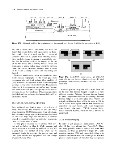
7000 Å 3000 Å 8000 Å 13000 Å 4000 Å 9000 Å
Planarized
M1
oxide
M1 Interlevel M1 M1
Poly-Si Interlevel M1
M1 Poly-Si
Field oxide + +
N OR P
Active area
Figure 27.2 Via-depth problem due to planarization. Reproduced from Brown, D. (1986), by permission of IEEE
via hole is often critical. Fortunately, via holes are
larger than contact holes, and aspect ratios are there-
fore smaller (but they need not be, if intermetal
dielectric thickness is greater than interpoly dielec-
tric). Via hole etching is similar to contact-hole etch-
(a) (b)
ing, but the etching needs to be stopped at the top
of the first metal, and selectivity between oxide and
aluminium is much higher than selectivity between
oxide and silicon. However, because there is metal
on the wafer, cleaning solutions after via etching are
limited. (c)
Two-level metallization cannot be extended to three
Figure 27.3 Oxide-CMP planarization: (a) (PE)CVD
levels because topography of the wafer gets more
oxide fills the gap between aluminium lines; (b) blind
pronounced after each level, and gap-filling capability of
polishing of oxide (no end point) and (c) second CVD oxide
(PE)CVD dielectric deposition as well as sputtering step
deposition
coverage in via holes will hit the limits. Planarization
helps, but it is no panacea: the surface may become
flat, which eliminates optical lithography depth-of-focus Backend process integration differs from front end
problems but, as shown in Figure 27.2, creates problems in the sense that thermal budget concept has a very
in via-hole etching and sputtering because holes will be different meaning. Whereas front-end thermal budget
of different depths. is about temperature-diffusion relationship, backend
thermal budget is about temperature-stress relation. For
n-level metallization there will be 2n steps at 300 to
27.2 MULTILEVEL METALLIZATION 400 C (one CVD tungsten and one PECVD dielectric
◦
deposition for each layer), with room temperature
True multilevel metallization starts at three levels of steps (etching, spin coating, CMP) in between. Stress,
metal. Historically, this occurred in the late 1980s strain, adhesion, hillocks, voids and cracks have to be
when submicron CMOS technologies were introduced. understood.
In 0.25 µm technology, up to six levels of metal are used
in ASICs and logic chips and three levels in memory
chips. It is expected that in 65 nm technology generation, 27.2.1 Contact/via plug
there can be ten levels of metal.
A fully planar structure can be created when con- In order to get planarized metallization, CVD W-
tact and via holes are filled by CVD tungsten, and plug fill has been adopted (see Figure 20.7). There
excess tungsten is removed, by etchback or by CMP are many possible routes to achieve the same final
(Figure 20.7). The number of metal levels can be structure, and they are pictured in Figure 27.4. Both
increased simply by repeating the process over and selective tungsten CVD and contact-hole filling with
over again because the topography does not change sputtered aluminium would be advantageous from the
(Figures 16.1 and 27.3). process simplicity point of view, but they have proven