
Page 304 - Sami Franssila Introduction to Microfabrication
P. 304
Multilevel Metallization 283
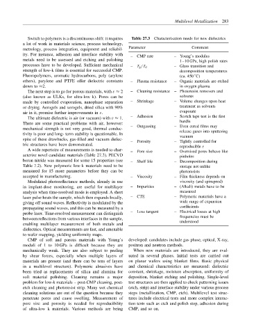
Switch to polymers is a discontinuous shift: it requires Table 27.3 Characterization needs for new dielectrics
a lot of work in materials science, process technology,
Parameter Comment
metrology, process integration, equipment and reliabil-
ity. For instance, adhesion and interface stability with
– CMP rate – Young’s modulus
metals need to be assessed and etching and polishing 1–10 GPa, high polish rates
processes have to be developed. Sufficient mechanical – T g /T d – Glass transition and
strength of low-k films is essential for successful CMP. decomposition temperatures
Fluoropolymers, aromatic hydrocarbons, poly (arylene (ca. 450 C)
◦
ethers), parylene and PTFE offer dielectric constants – Plasma resistance – Organic materials are etched
down to ≈2. in oxygen plasma
The next step is to go for porous materials, with ε ≈ 2 – Cleaning resistance – Photoresist removers and
(also known as ULKs, for ultra-low k). Pores can be solvents
made by controlled evaporation, nanophase separation – Shrinkage – Volume changes upon heat
or drying. Aerogels and xerogels, dried silica with 90% treatment as solvents
air in it, promise further improvements in ε. evaporate
The ultimate dielectric is air (or vacuum) with ε ≈ 1. – Adhesion – Scotch tape test is the first
There are some practical problems with air, however: hurdle
mechanical strength is not very good, thermal conduc- – Outgassing – Even cured films may
release gases into sputtering
tivity is poor and long- term stability is questionable. In vacuum
spite of these drawbacks, gas-filled and vacuum dielec- – Porosity – Tightly controlled for
tric structures have been demonstrated.
reproducible ε
A wide repertoire of measurements is needed to char- – Pore size – Oversized pores behave like
acterize novel candidate materials (Table 27.3). PECVD pinholes
boron nitride was measured for some 15 properties (see – Shelf life – Decomposition during
Table 7.2). New polymeric low-k materials need to be storage not unlike
measured for 15 more parameters before they can be photoresists
accepted in manufacturing. – Viscosity – Film thickness depends on
Modulated photoreflectance methods, already in use viscosity (and spinspeed)
in implant-dose monitoring, are useful for multilayer – Impurities – (Alkali) metals have to be
analysis when time-resolved mode is employed. A short measured
laser pulse heats the sample, which then expands locally, – CTE – Polymeric materials have a
giving off sound waves. Reflectivity is modulated by the wide range of expansion
propagating sound waves, and this can be measured by a coefficients
probe laser. Time-resolved measurement can distinguish – Loss tangent – Electrical losses at high
between reflections from various interfaces in the sample, frequencies must be
enabling multilayer measurement of both metals and understood
dielectrics. Optical measurements are fast, and amenable
to wafer mapping, yielding uniformity maps.
CMP of soft and porous materials with Young’s developed: candidates include gas phase, optical, X-ray,
moduli of 1 to 10 GPa is difficult because they are positron and neutron methods.
mechanically weak. They are also subject to peeling When new materials are introduced, they are eval-
by shear forces, especially when multiple layers of uated in several phases. Initial tests are carried out
materials are present (and there can be tens of layers on planar wafers using blanket films. Basic physical
in a multilevel structure). Polymeric abrasives have and chemical characteristics are measured: dielectric
been tried as replacements of silica and alumina for constant, shrinkage, moisture absorption, uniformity of
soft material polishing. Cleaning remains a major deposition, blanket etching and polishing. Single-level
problem for low-k materials – post-CMP cleaning, post- test structures are then applied to check patterning issues
etch cleaning and photoresist strip. Many wet chemical (etch, strip) and interface stability under various process
cleaning solutions are out of the question because they steps (metallization, CMP, etch). Multilevel test struc-
penetrate pores and cause swelling. Measurement of tures include electrical tests and more complex interac-
pore size and porosity is needed for reproducibility tion tests such as etch and polish stop, adhesion during
of ultra-low k materials. Various methods are being CMP, and so on.