
Page 309 - Sami Franssila Introduction to Microfabrication
P. 309
288 Introduction to Microfabrication
Many processes take place on all surfaces in the reac-
tor. The films or doping structures on the wafer backside
are often of poor quality because most processes are
optimized for the front side alone. If single-side polished
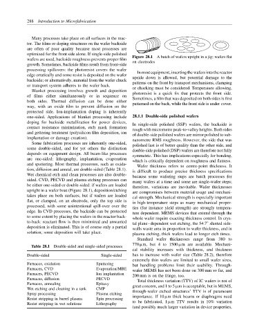
wafers are used, backside roughness prevents proper film Figure 28.1 A batch of wafers upright in a jig; wafers flat
on electrodes
growth. Sometimes, backside films result from front-side
processing spillovers: the photoresist covers the wafer
edge erratically and some resist is deposited on the wafer In most equipment, inserting the wafers into the reactor
backside; or alternatively, material from the wafer chuck upside down is allowed, but potential damage to the
or transport system adheres to the wafer back. patterns on the front by transport mechanisms, clamping
Blanket processing involves growth and deposition or chucking must be considered. Temperature allowing,
of films either simultaneously or in sequence on photoresist is a quick fix that protects the front side.
Sometimes, a film that was deposited on both sides is first
both sides. Thermal diffusion can be done either patterned on the back, while the front side is under cover.
way, with an oxide film to prevent diffusion on the
protected side. Ion-implantation doping is inherently
one-sided. Applications of blanket processing include 28.1.1 Double-side polished wafers
doping for backside metallization for power devices, In single-side polished (SSP) wafers, the backside is
contact resistance minimization, etch mask formation rough with micrometre peak-to-valley heights. Both sides
and gettering treatment (polysilicon film deposition, ion of double-side polished wafers are mirror polished to sub-
implantation or damage creation). nanometre RMS roughness. However, the side that was
Some fabrication processes are inherently one-sided, polished last is of better quality than the other side, and
some double-sided, and for yet others the distinction double-side polished (DSP) wafers are therefore not fully
depends on equipment design. All beam-like processes symmetric. This has implications especially for bonding,
are one-sided: lithography, implantation, evaporation which is critically dependent on roughness and flatness.
and sputtering. Most thermal processes, such as oxida- Wafer thickness refers to centre-point thickness. It
tion, diffusion and anneal, are double-sided (Table 28.1). is difficult to produce precise thickness specifications
Wet chemical etch and clean processes are also double- because some wafering steps are batch processes for
sided. CVD, PECVD and plasma etching processes can many wafers at a time and some are single-wafer steps;
be either one-sided or double-sided: if wafers are loaded therefore, variations are inevitable. Wafer thicknesses
upright in a wafer boat (Figure 28.1), deposition/etching are compromises between material usage and mechani-
takes place on both surfaces, but if wafers are loaded cal strength. Mechanical strength is especially important
flat, or clamped, on an electrode, only the top side is in high-temperature steps as many mechanical proper-
processed, with some unintentional spill-over over the ties (for instance yield strength) are strongly tempera-
edge. In CVD processes, the backside can be protected ture dependent. MEMS devices that extend through the
to some extent by placing the wafers in the reactor back- whole wafer require exacting thickness control. In crys-
to-back: reactant flow is then minimized and unwanted tal plane–dependent wet etching, the 54.7 slanted side-
◦
deposition is eliminated. This is of course only a partial walls waste area in proportion to wafer thickness, and in
solution; some deposition will take place. plasma etching, thick wafers lead to longer etch times.
Standard wafer thicknesses range from 380 to
770 µm, but 4 to 1500 µm are available. Mechani-
Table 28.1 Double-sided and single-sided processes
cal stability increases with thickness, and thickness
Double-sided Single-sided has to increase with wafer size (Table 28.2), therefore
extremely thin wafers are limited to small wafer sizes,
Furnaces, oxidation Sputtering but handling problems limit their usability. Through-
Furnaces, CVD Evaporation/MBE
wafer MEMS has not been done on 300 mm so far, and
Furnaces, PECVD Ion implantation 200 mm is on the fringe, too.
Furnaces, diffusion PECVD
Total thickness variation (TTV) of IC wafers is not of
Furnaces, annealing Epitaxy great concern, and 1 to 5 µm is acceptable, but in MEMS,
Wet etching and cleaning in a tank CMP
Spray processing Plasma etching through-wafer etched structures’ TTV is of paramount
Resist stripping in barrel plasma Spin processing importance. If 10 µm thick beams or diaphragms need
Resist stripping in wet solutions Lithography to be fabricated, 1 µm TTV results in 10% variation
(and possibly much larger variation in device properties,